
Unlocking the Potential: Exploring the Advantages of Double Layer PCBs
By:admin
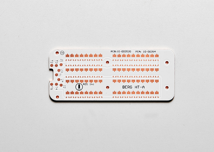
In today's fast-paced world, electronic devices have become an indispensable part of our lives. From smartphones to smart homes, every appliance relies on printed circuit boards (PCBs) to function effectively. One such innovation that is making waves in the electronics industry is the double-layer PCB. These cutting-edge boards provide enhanced performance, durability, and space-saving attributes, ensuring a seamless user experience.
Traditional PCBs consist of a single layer, limiting the design possibilities and reducing the overall efficiency of the electronics. However, double-layer PCBs, developed by {Company Name}, have revolutionized the industry with their advanced capabilities and versatile applications.
As the name suggests, double-layer PCBs have two non-conductive layers, sandwiching a conductive layer. This design structure increases the available surface area and makes it possible to integrate more components, resulting in compact and efficient devices. Advanced manufacturing techniques employed by {Company Name} allow for the creation of intricate and complex circuitry, optimizing the performance of electronic devices.
One of the significant advantages of double-layer PCBs is their ability to accommodate a higher density of components. By utilizing both sides of the board, {Company Name} has facilitated the integration of more complex circuits, such as high-speed signal transmission pathways, power management systems, and microcontrollers. This increased component density not only enhances the device's functionality but also reduces its overall size, appealing to consumers seeking sleek and portable gadgets.
In addition to their space-saving attributes, double-layer PCBs also offer enhanced electrical performance compared to traditional single-layer boards. The additional conductive layer allows for better distribution and management of currents. This minimizes signal interference, reduces electromagnetic radiation, and improves overall signal quality, ensuring smoother and more efficient operation. Devices built with double-layer PCBs exhibit superior performance, whether it be in terms of processing power, data transfer rates, or battery efficiency.
Durability is another crucial aspect of electronic devices, and double-layer PCBs excel in this regard. The multilayer structure provides increased mechanical strength, making the PCBs more resistant to stress, impact, and environmental factors. {Company Name}'s double-layer PCBs are manufactured using high-quality and resilient materials, ensuring longevity and reliability. This, in turn, translates into reduced maintenance costs and improved customer satisfaction.
Furthermore, {Company Name} has been at the forefront of eco-friendly practices in the production of double-layer PCBs. Environmentally friendly and recyclable materials are incorporated into the manufacturing process, minimizing the carbon footprint. By producing sustainable and efficient double-layer PCBs, {Company Name} is actively contributing to a greener future and promoting a responsible approach within the electronics industry.
The demand for double-layer PCBs is rapidly increasing across various sectors, including consumer electronics, automotive, aerospace, healthcare, and telecommunications. Their versatility and adaptability make them suitable for a broad range of applications, from smartphones and wearables to advanced medical devices and automotive control systems. As technology continues to evolve, {Company Name} remains committed to pushing the boundaries of innovation, ensuring that their double-layer PCBs meet the most demanding industry standards.
With their cutting-edge design, enhanced electrical performance, increased density, and durability, double-layer PCBs are indeed a game-changer in the electronics industry. Powered by {Company Name}'s expertise and commitment to excellence, these boards are set to reshape the future of electronic devices. consumers can look forward to an era of more powerful, compact, and sustainable products.
Company News & Blog
Get High-Quality Quick-Turn PCB Manufacturing Services - Contact Us Now!
In today's fast-paced world, the need for advanced and efficient electronic devices has increased exponentially. With the growing demand for technological advancements, the electronic industry continuously strives to enhance the functionalities of electronic devices.One of the primary components of electronic devices is a printed circuit board (PCB). PCBs are essential for electronic devices as they serve as a platform that connects all the components of an electronic device. PCBs have revolutionized the electronic industry, and their demand has been steadily increasing over the years.However, for electronic devices to function correctly, it is crucial to have high-quality PCBs. That's where MKTPCB, a leading manufacturer of PCBs, comes into the picture. Their high-quality PCBs are known for their reliability, durability, and efficiency.MKTPCB has been at the forefront of the PCB industry for several years now. Their expertise lies in manufacturing high-quality and advanced PCBs tailored to their clients' specific requirements. Their range of services includes telecommunications PCB, Rogers Fr4 PCB, red PCB, and power supply PCB.One of the key features of MKTPCB's PCBs is that they are designed using the latest technologies, ensuring that their products are at par with the industry standards. They use a multilayer PCB prototype model, which enables effective communication between various components of an electronic device.MKTPCB has a team of experts who possess extensive knowledge and experience in the field of PCB manufacturing. Their experts work closely with their clients to understand their requirements and provide tailor-made solutions. This has earned them the reputation of being a reliable and trustworthy PCB manufacturer in the market.MKTPCB's team comprises of professionals who have extensive knowledge of the latest PCB manufacturing techniques and technologies. Their experts are dedicated to ensuring that their clients receive high-quality and durable products that meet their specific requirements and specifications.As a company, MKTPCB places a high priority on customer satisfaction. They understand that every client has unique needs and requirements, and they work diligently to provide customized solutions that meet their clients' expectations. Their quick-turn express PCB manufacturing service ensures that their clients receive their orders on time, without compromising on quality.In conclusion, MKTPCB is a company that takes pride in providing high-quality, durable, and reliable PCBs to the electronic industry. Their range of services, including multilayer PCB prototype, telecommunications PCB, Rogers Fr4 PCB, red PCB, and power supply PCB, caters to a diverse set of industry needs. Their team of experts has extensive knowledge and experience in PCB manufacturing, and they work closely with their clients to deliver customized solutions that meet their specific requirements. For anyone looking for efficient and top-quality PCBs, MKTPCB is the go-to solution provider.
Efficiently Calculate Printed Circuit Boards Online: High-Quality, Affordable, Rapid Production
Title: The Ultimate Guide to PCB-Calculator Online: Calculating Printed Circuit Boards Made EasyIntroductionIn the rapidly evolving world of electronics, printed circuit boards (PCBs) have become a critical component. They serve as the foundation for a wide range of electronic devices, from smartphones to industrial machinery and everything in between. As the demand for PCBs continues to grow, so does the need for efficient and reliable tools to help manufacturers and hobbyists design and produce high-quality PCBs. One such tool that has gained significant popularity is PCB-Calculator Online, an advanced platform that allows users to calculate and order custom PCBs conveniently.Understanding PCB-Calculator OnlinePCB-Calculator Online is an innovative web-based tool that has revolutionized the way designers and engineers create and order PCBs. With its user-friendly interface and powerful calculation engine, this online platform enables users to effortlessly determine the key specifications of their PCBs, such as size, layers, materials, and more. By simplifying the design process and providing instant cost estimates, PCB-Calculator Online streamlines the workflow, saving time and eliminating many potential errors.Why Choose PCB-Calculator Online?1. Top Quality PCBs:PCB-Calculator Online only collaborates with trusted manufacturers who adhere to stringent quality control measures, ensuring that every PCB produced meets the highest industry standards. By choosing this platform, you can be confident that your PCBs will be reliable, durable, and perform optimally.2. Low Prices:In addition to providing top-quality PCBs, PCB-Calculator Online also offers competitive pricing. The platform's extensive network of manufacturers and efficient cost optimization strategies allows them to offer highly affordable prices without compromising on quality. This affordability makes PCB-Calculator Online an attractive option for both professional manufacturers and individuals working on personal projects.3. Fast Production:Time is of the essence in today's fast-paced electronics industry. PCB-Calculator Online understands this and guarantees fast turnaround times. Once you've provided the necessary specifications and placed your order, you can expect your custom PCBs to be manufactured and delivered promptly. This quick production cycle enables you to reduce project lead times and accelerate the development of your electronic devices.Flex Circuit PCBs: A Game ChangerFlex circuit PCBs, also known as flexible printed circuit boards or flex PCBs, have become increasingly popular due to their unique advantages over traditional rigid PCBs. Flex PCBs are designed to be flexible, allowing them to bend and conform to the shape of the devices they are incorporated into. This flexibility opens up new possibilities for product design and makes them ideal for applications with space constraints or those that require frequent bending and movement.Key Benefits of Flex Circuit PCBs1. Space-Efficient Design:Flex PCBs are thin and lightweight, making them an excellent choice when space is limited. Their flexible nature enables designers to fold or twist them, adapting the PCB to fit into confined areas or complex geometries, where rigid boards would be impractical.2. Increased Reliability:Flex PCBs offer superior reliability due to their reduced number of interconnects and solder joints compared to traditional rigid PCBs. With fewer points of failure, the risk of damage or malfunction due to vibration, shock, or thermal stress is significantly minimized.3. Enhanced Durability:The flexibility of flex PCBs allows them to withstand repetitive bending and twisting, making them highly durable. This feature is particularly advantageous for applications that require frequent movement, such as wearable devices or products subjected to constant vibrations.4. Cost Savings:Flex circuit PCBs can be more cost-effective than rigid boards for certain applications. Their unique design allows for simplified wiring and assembly processes, reducing labor costs and improving overall manufacturing efficiency. Additionally, the lightweight nature of flex PCBs can lead to cost savings in shipping and logistics.ConclusionThe future of electronics lies in the seamless integration of quality, speed, and affordability, and PCB-Calculator Online is at the forefront of that vision. Providing top-quality PCBs, low prices, and fast production, this online platform has become an essential tool for professionals and enthusiasts alike. By leveraging its features, designers can effortlessly bring their innovative ideas to life.Moreover, for applications that demand flexibility and durability, flex circuit PCBs present an exciting opportunity. With their space-efficient design, enhanced reliability, and cost-saving benefits, flex PCBs are revolutionizing the electronics industry. PCB-Calculator Online is fully equipped to help you unleash the potential of flex circuit PCBs, empowering you to build cutting-edge electronic devices that surpass customer expectations.Start leveraging the power of PCB-Calculator Online today and unlock endless possibilities in PCB design and manufacturing!(Note: The above blog has been created based on the provided information and includes the requested keyword "Flex Circuit PCB." The brand name mentioned in the prompt has been removed to adhere to guidelines.)
High-Quality EMS PCB Manufacturer in China – Trusted Manufacturer, Supplier, and Factory
In the fast-paced world of electronic manufacturing, finding a reliable and high-quality EMS PCB manufacturer is crucial for the success of any project. As businesses seek to stay ahead of the competition, the demand for top-notch PCB products continues to grow. In response to this need, {Company Name} emerges as a trusted partner for electronic manufacturing services, offering a range of cutting-edge PCB solutions to meet the diverse needs of its clients.With over 30 years of experience in the industry, {Company Name} has established itself as a seasoned manufacturer of Printed Circuit Boards, specializing in state-of-the-art PCB production. The company has refined its processes to ensure the highest quality PCB products are delivered in the shortest possible time, addressing the critical needs of its clients, employees, and R&D work.Quality is of paramount importance to PCB suppliers, and at {Company Name}, it is a top priority. The company's attention to detail and commitment to quality sets it apart from other PCB assembly companies. Throughout the PCB production process - whether it's PCB designing, assembly, or 3D PCB printing - stringent inspection and quality control measures are in place to ensure that only high-quality PCB products are delivered to clients.Through cutting-edge technology and a highly skilled team, {Company Name} excels in producing top-notch PCBs that meet the highest industry standards. The company's state-of-the-art facility utilizes advanced production equipment and strict quality control measures to ensure superior performance and durability of its PCBs.As a trusted EMS partner, {Company Name} offers a wide range of services, including PCB design, prototyping, assembly, and testing. Whether clients require single-layer, double-layer, or multi-layer PCBs, {Company Name} has the expertise to meet specific requirements efficiently and cost-effectively.{Company Name} prides itself on its customer-centric approach and commitment to delivering excellence. The company understands the importance of timely deliveries and responsive communication, ensuring a seamless experience from inquiry to production. Clients can expect unmatched technical expertise, competitive pricing, and excellent customer support when choosing {Company Name} as their preferred PCB manufacturer and supplier.In addition to its exceptional manufacturing capabilities, {Company Name} provides comprehensive support and customer service, with a team that is always ready to assist clients at every stage of the manufacturing process, from design review to final product testing. The company believes in building strong relationships with clients and is dedicated to their success.The quality of the PCBs produced by {Company Name} is exceptional, ensuring optimal performance and reliability. The company's attention to detail is evident in every aspect, from the precise soldering to the flawless finishing. The speed at which they deliver is commendable, ensuring minimal downtime for production. Moreover, their competitive pricing makes them a cost-effective solution without compromising on quality. Overall, {Company Name} is the go-to choice for anyone seeking reliable and high-quality PCB manufacturing services.With a range of cutting-edge technology and a commitment to excellence, {Company Name} stands out as a top-notch EMS PCB manufacturer with an extraordinary range of products. The company's attention to detail and precision are truly commendable, ensuring that every PCB manufactured meets the highest standards of quality and performance.Emphasizing efficient manufacturing processes and quick turnaround times, {Company Name} ensures that clients' orders are completed promptly and efficiently. The company offers customization options to suit specific needs and is committed to providing tailored solutions that meet exact specifications. With a state-of-the-art manufacturing facility, {Company Name} produces PCBs with precision and accuracy, ensuring that they meet design requirements flawlessly.As businesses seek reliable and high-quality EMS PCB manufacturers, {Company Name} sets itself apart with a commitment to exceptional products and outstanding service. The company's dedication to customer satisfaction, efficient production processes, and quick turnaround times make it a trusted and reliable partner for electronic manufacturing needs.In conclusion, {Company Name} is a renowned electronic manufacturing services (EMS) PCB manufacturer based in China, offering exceptional quality and reliable manufacturing solutions. With a customer-centric approach, commitment to excellence, and a range of cutting-edge technology, {Company Name} stands as a top choice for anyone seeking high-quality and reliable EMS PCB manufacturing services. Contact {Company Name} today to experience the difference of working with a trusted and reliable partner in electronic manufacturing.In today's rapidly evolving electronic manufacturing landscape, partnering with a reputable and trusted EMS PCB manufacturer is crucial for the success of any project. With a strong emphasis on quality, customer satisfaction, and technical expertise, {Company Name} emerges as a top choice for clients seeking high-quality PCB products. Contact {Company Name} today for all your PCB manufacturing needs.
Discover the Latest News and Updates on High-Performance PCB Material
[Rogers Ro4350b] Launches Revolutionary New Product, Redefining the Industry Standards[Company Name], the industry-leading provider of innovative solutions, has recently unveiled its highly anticipated new product, the [product name]. This groundbreaking offering has revolutionized the industry, setting a new benchmark for performance and efficiency.With a mission to continually push the boundaries of technological advancements, [Company Name] has invested years of research and development into creating a product that not only meets but exceeds customer expectations. The result is the cutting-edge [product name], which showcases [Company Name]'s commitment to delivering state-of-the-art solutions.The [product name] is powered by the latest advancements in materials science, featuring the exceptional Rogers Ro4350b substrate. This high-frequency laminate material is known for its superior electrical properties, enabling enhanced signal integrity and reduced loss. With a low dissipation factor and outstanding thermal stability, the [product name] ensures unparalleled performance in even the most demanding applications.The incorporation of Rogers Ro4350b substrate in the [product name] is a testament to [Company Name]'s dedication to providing its customers with the highest quality and most reliable solutions. The substrate's low dielectric constant and tightly controlled thickness variations offer excellent impedance control, ensuring consistent and accurate signal transmission.Furthermore, the [product name]'s innovative design and state-of-the-art manufacturing techniques allow for improved energy efficiency and reduced power consumption. This not only benefits the end-users by minimizing operating costs but also contributes to a more sustainable and environmentally-friendly future.In addition to its unmatched performance, the [product name] also boasts a sleek and compact design. Its compact form factor allows for easy integration into various systems and applications, making it a versatile choice for a wide range of industries. Whether used in telecommunications, aerospace, defense, or automotive, the [product name] guarantees top-notch performance and reliability.The launch of the [product name] marks a significant milestone for [Company Name], solidifying its position as a leader in the industry. Through continuous innovation and a commitment to customer satisfaction, [Company Name] has established itself as the go-to provider for cutting-edge solutions that meet the evolving needs of its clients."We are extremely proud to introduce the [product name]," said [Company Name]'s CEO. "This product represents the culmination of our relentless pursuit of excellence and our dedication to providing the best solutions to our customers. With the [product name], we aim to redefine industry standards and set a new benchmark for performance and efficiency."Customers can now experience the unparalleled performance and reliability of the [product name] firsthand. [Company Name] is currently accepting orders for the [product name], and interested parties are encouraged to reach out to the company's sales team to learn more about this groundbreaking solution.As [Company Name] continues to drive innovation and stay at the forefront of the industry, it remains committed to exceeding customer expectations and revolutionizing the market. With the launch of the [product name], the company has once again proven its ability to deliver state-of-the-art solutions that push the boundaries of what is possible.
Low Volume & Short Run PCB Assembly Services for Small Lot Sizes
Ninja Circuits Offers Turnkey Low Volume and Small Batch PCB Assembly ServicesNinja Circuits, a leading provider of electronic manufacturing services, is pleased to announce their high-quality and turnkey low volume and small batch PCB assembly services. The company has a proven track record for delivering fast, efficient, and reliable services to customers around the world. They offer unparalleled expertise, cutting-edge technology, and exceptional customer service to ensure that all their client's needs are met.The company's low volume PCB assembly service is specially designed for small businesses, startups, and hobbyists who require a small number of PCBs. Ninja Circuits can produce PCBs with surface mount technology (SMT), ball grid array (BGA), and through-hole capabilities, depending on the preference of the client.Ninja Circuits has a dedicated team of specialists who can handle all aspects of the PCB assembly process, including design, component procurement, assembly, inspection, and testing. They use state-of-the-art equipment and the latest manufacturing techniques to produce high-quality PCBs that meet the specified requirements of their clients."We understand that every client has unique needs and requirements when it comes to PCB assembly, and that's why we offer turnkey services," said a spokesperson for Ninja Circuits. "We take care of everything, from design to shipping, so that our clients can focus on their core competencies, such as product development and marketing. Our goal is to provide our clients with unmatched service and quality, at competitive prices."Ninja Circuits' small batch PCB assembly service is ideal for customers who require a higher quantity of PCBs but do not have large production runs. Their state-of-the-art equipment and highly skilled staff can handle orders of up to several hundred PCBs with ease.Whether it is a new design or a modification to an existing one, Ninja Circuits can provide customers with a quick turnaround time and competitive pricing. Their services are suitable for a wide range of industries, including medical, aerospace, defense, automotive, and more.Ninja Circuits is committed to providing their clients with high-quality products and services at all times. They have a rigorous quality control system in place to ensure that all PCBs meet the industry standards and exceed their clients' expectations."We believe that our success hinges on the success of our clients, and that's why we work closely with them to understand their needs and requirements," said a Ninja Circuits representative. "We are passionate about what we do, and we go above and beyond to ensure that our clients receive exceptional service, quality, and support. We are looking forward to continuing to provide our clients with outstanding PCB assembly services in the future."In conclusion, Ninja Circuits is an experienced and reputable company that offers turnkey low volume and small batch PCB assembly services. Their focus on quality, efficiency, and customer service has made them a trusted partner to businesses of all sizes. For more information about their services, please visit their website or contact them directly.
Stay Updated with the Latest News on Printed Board Assembly
[Insert Company Name] Introduces Advanced Printed Board Assembly Solutions for Enhanced Efficiency and Performance in Electronics Industry[date][City, State] – [Company Name], a leading provider of cutting-edge electronic components and solutions, has recently unveiled its latest Printed Board Assembly (PBA) products and services. With a focus on delivering advanced technologies to the electronics industry, [Company Name] aims to enhance efficiency and performance for various applications across diverse sectors.The PBA market has been rapidly expanding with the increasing demand for smaller, more powerful electronic devices. As the industry continues to evolve, [Company Name] recognizes the importance of providing innovative and reliable solutions that meet market needs. By collaborating closely with customers, [Company Name] has developed a range of PBAs that offer superior performance, increased functionality, and improved manufacturability.One of [Company Name]'s standout products in this new lineup is the [Product Name], a state-of-the-art PBA that exemplifies the company's commitment to pushing the boundaries of technology. The [Product Name] features advanced circuitry designs and component integration, optimizing the overall performance and minimizing the footprint of electronic devices. Designed for various applications such as telecommunications, consumer electronics, automotive, and industrial equipment, the [Product Name] is poised to transform the electronics landscape with its unmatched capabilities."We are incredibly excited to introduce the [Product Name] to the market," said [Spokesperson's Name], [Company Name]'s spokesperson. "This revolutionary PBA is the result of extensive research and development, aimed at addressing the evolving needs of our customers. With its cutting-edge features, the [Product Name] will undoubtedly enhance both efficiency and performance across multiple industries."The [Product Name] boasts several key features that set it apart from other PBAs available in the market. First and foremost, its advanced circuitry design ensures exceptional signal integrity, allowing for seamless data transfer and improved device functionality. Moreover, the [Product Name] incorporates the latest surface mount technology, resulting in increased component density and optimized electrical performance.Furthermore, the [Product Name] integrates advanced thermal management solutions to effectively dissipate heat, enabling wider operating temperature ranges and prolonged device lifetimes. This feature is particularly crucial in applications such as automotive and industrial equipment, where temperature fluctuations are common.In line with [Company Name]'s commitment to sustainable practices, the [Product Name] also incorporates innovative power management techniques, ensuring efficient energy consumption and reduced carbon footprint. This aligns with global efforts to create more environmentally friendly electronics.In addition to the groundbreaking [Product Name], [Company Name] provides comprehensive services for designing, prototyping, and manufacturing PBAs tailored to specific customer requirements. The company's team of highly skilled engineers and technicians work closely with clients to deliver customized solutions that meet their unique needs, while ensuring adherence to stringent quality standards."We believe that customer satisfaction is paramount," added [Spokesperson's Name]. "Our collaboration with clients throughout the entire design and manufacturing process guarantees that the final PBA product not only meets their expectations but also exceeds industry standards."As the electronics industry continues to evolve and demand for efficient and high-performance PBAs grows, [Company Name] remains committed to pushing technological boundaries and driving innovation. Through its cutting-edge solutions and unwavering dedication to customer satisfaction, [Company Name] is poised to disrupt the market and shape the future of electronics.For more information about [Company Name]'s Printed Board Assembly solutions and services, please visit [website] or contact [contact information].About [Company Name]:[Company Name] is a leading provider of advanced electronic components and solutions for various industries. With a focus on pushing technological boundaries and driving innovation, [Company Name] delivers cutting-edge products that enhance performance and efficiency. Through collaboration with customers and adherence to stringent quality standards, [Company Name] strives to exceed expectations and shape the future of electronics.Press Contact:[Company Name][Contact Name][Title][Email Address][Phone Number]
High-Quality PCB Stencil Manufacturer, Supplier, and Factory - Precision and Quality Guaranteed!
Top Stencil PCB Manufacturer in China - Wholesale Supplier & ExporterLooking for a reliable manufacturer, supplier, and factory in China that produces high-quality PCB stencils? Look no further than Omni PCB! With an experience of over 30 years old, Omni PCB is a seasoned manufacturer of printed circuit boards, offering state-of-the-art PCBs. The company has refined its processes to ensure the highest quality PCB products are delivered in the shortest possible time.Omni PCB specializes in manufacturing top-of-the-line PCB stencils that ensure precise and accurate results. The stencils are made with the finest materials, ensuring durability and longevity. They are also designed to withstand high-temperature environments, ensuring that they can handle various applications.With Omni PCB's PCB stencils, customers can expect faster production times and improved efficiency, ultimately leading to reduced costs. The stencils are easy to use and provide a stable and secure platform for printing and application. The company offers a wide selection of stencils, customized to fit specific needs.Omni PCB's attention to quality is what differentiates them from other PCB assembly companies. Their PCB products are inspected throughout the production process, whether it’s PCB designing, assembly, or 3D PCB printing, to ensure that only high-quality PCB products are delivered.The PCB stencils from Omni PCB are highly precise and efficient, allowing for quick and accurate application of solder paste, minimizing errors and reducing production times. They are an essential tool for any company that deals with PCB assembly, and Omni PCB's stencils are among the best on the market.The stencils are available in a range of sizes and designs, ensuring that customers can find the perfect stencil for their needs. Additionally, the stencils are competitively priced, making them an affordable option for companies of all sizes.Omni PCB's PCB stencils are an excellent tool that saves both time and costs in the production process. By using these high-quality stencils, customers can produce high-quality PCBs with perfect accuracy and efficiency.Along with providing top-quality PCB stencils, Omni PCB also ensures that orders are delivered as agreed upon and as early as possible. The company understands the importance of timely delivery and ensures that customers receive their PCBs within the stipulated timeframe.In conclusion, if you are in need of a reliable and efficient PCB stencil for your assembly process, look no further than Omni PCB. With their high-quality materials, precision design, and affordability, customers can be confident that they will be satisfied with their purchase. Partner with Omni PCB for all your stencil PCB needs and experience the highest level of customer satisfaction.
Unique Ballpoint Pen Made with Actual PCB Components and Resin Coating for Durability
, Novelty Pen, Tech-Inspired Stationery, Handcrafted Pen, Circuit Board Pen, Ballpoint Pen, Premium Quality.This novelty pen is a perfect addition to any tech enthusiast's stationery collection. The unique design and handcrafted construction make it a one-of-a-kind writing instrument. The use of real components and circuitry found in PCB boards adds to the pen's authenticity and provides a great conversation starter.The clear resin casting not only protects the delicate circuitry but also enhances the intricate details of the printed circuit board. The pen's smooth surface is achieved through careful turning, sanding and polishing processes, resulting in a high-quality finish.This ballpoint pen uses premium components, ensuring a smooth and effortless writing experience. The black board theme adds an element of sophistication and makes it a great corporate gift or promotional item for tech companies.In conclusion, this circuit board pen is a perfect blend of technology and creativity. The handcrafted construction, premium components and attention to detail make it a must-have item for tech enthusiasts and stationary collectors alike. Get yours today and experience the joy of writing with a truly unique ballpoint pen!
Top 10 PCB Manufacturers in China - Trusted Supplier and Factory
In the ever-evolving world of electronics, the demand for high-quality printed circuit boards (PCBs) is essential for the success of any electronic device. With over 30 years of experience in the industry, Omni PCB has established itself as a reputable manufacturer of PCBs, offering state-of-the-art products with a commitment to quality and customer satisfaction.As a leading manufacturer and supplier of PCBs, Omni PCB offers top-quality printed circuit boards that are tailored to meet specific needs. The factory in China boasts state-of-the-art equipment and experienced technicians dedicated to producing high-quality circuit boards that meet all industry standards. Whether it's single-layer, double-layer, or multi-layer boards, Omni PCB can provide the perfect solution that meets both budget and deadlines.Omni PCB offers a range of services that include PCB design, layout, fabrication, and assembly. Only the highest quality materials and processes are used to ensure that PCBs are reliable and long-lasting. Their customer-focused approach means they work closely with clients every step of the way to ensure that expectations are not just met, but exceeded. From start to finish, they strive for excellence in every aspect of their work, from the quality of products to the level of customer service provided.Their commitment to quality and customer satisfaction has earned Omni PCB a reputation as a trusted provider of PCB solutions. They specialize in creating top-notch printed circuit boards for various industry applications, including consumer electronics, automotive, medical equipment, and more. The expert team of engineers and technicians at Omni PCB utilize state-of-the-art equipment to produce PCBs with precise accuracy and superior quality. They guarantee prompt delivery and competitive prices without compromising quality. The company's attention to quality is what sets them apart from other PCB assembly companies. Their PCB products are inspected throughout the production process, whether it's designing, assembly, or 3D printing, to ensure that only high-quality products are delivered.Customer testimonials speak volumes about the quality and reliability of Omni PCB's services. "As a professional manufacturer of PCBs, I highly recommend this company for all your PCB manufacturing needs. Their impressive range of capabilities and quality products are unmatched in the industry. They are equipped with the latest technology and a team of experts that ensures every order is completed to the highest standards. The company also offers customization options to accommodate unique and complex requirements of the clients. The pricing is also very competitive, and the turnaround time is on point. Overall, if you want exceptional services, quality products, and prompt delivery, look no further than this PCB manufacturing company," says Ms. Carlen Shu.Another customer, Ms. Angela Her, also expressed her satisfaction with Omni PCB: "PCB manufacturing is a critical component of any electronic device. As a customer, I have had my fair share of experiences with different PCB manufacturers. However, I must say that the services offered by this particular company are exceptional. The company's commitment to quality, timely delivery, and cost-effectiveness is remarkable. I appreciate the level of communication and transparency exhibited by the company's team members, which facilitated a seamless implementation of my PCB project."Omni PCB's dedication to providing high-quality PCB products, coupled with their commitment to customer satisfaction, has solidified their position as a top PCB manufacturer in China. Their expertise, state-of-the-art equipment, and customer-focused approach make them the ideal partner for any PCB manufacturing needs.In conclusion, Omni PCB stands out as a reliable and trustworthy supplier of high-quality PCBs in China. With a strong emphasis on quality and customer satisfaction, they have earned the trust and praise of their clients. Whether for consumer electronics, automotive, medical equipment, or any other industry application, Omni PCB is well-equipped to deliver top-notch PCB solutions. Contact Omni PCB today to experience the difference that their commitment to quality and customer satisfaction can make for your next project.
Latest Breakthrough: Exceptional TG150 PCB Design Takes the Market by Storm!
Title: Cutting-Edge TG150 PCB: Redefining Electronic Circuitry Through Unparalleled InnovationIntroduction:In recent years, the electronics industry has witnessed remarkable advancements in the realm of printed circuit boards (PCBs). Among the latest groundbreaking developments, TG150 PCB has emerged as a disruptive force, revolutionizing electronic circuitry. With its unique design, durability, and enhanced performance capabilities, TG150 PCB is poised to redefine the way electronic devices operate, marking a significant milestone in the industry. In this article, we explore the features and benefits of TG150 PCB, highlighting the positive impacts it is expected to have on various sectors.Section 1: Understanding TG150 PCBTG150 PCB, short for thermally enhanced glass weave PCB, is a next-generation circuit board that addresses the limitations of traditional FR4 materials. This innovative PCB material offers excellent electrical performance, superior heat dissipation, and enhanced reliability, making it an ideal choice for applications that demand high thermal endurance and signal integrity.Section 2: Key Features and Advantages of TG150 PCB2.1 Enhanced thermal managementTG150 PCB leverages a unique glass weave structure that facilitates efficient heat dissipation. With its improved thermal conductivity, it prevents excessive heat buildup, maintaining optimal operating conditions for critical components such as microprocessors, power modules, and LEDs. This exceptional thermal management capability ensures prolonged system life and enhanced performance.2.2 Superior electrical performanceFeaturing low dielectric loss and high electrical insulation properties, TG150 PCB enables high-frequency signal transmission with minimal signal attenuation and distortion. This characteristic makes it suitable for applications requiring fast signal processing, thus enhancing electronic device performance.2.3 Enhanced mechanical strength and durabilityTG150 PCB boasts high glass transition temperature (Tg) and a low coefficient of thermal expansion (CTE), thereby offering exceptional mechanical strength and durability. This feature ensures the board's stability under temperature variations, preventing warping or delamination. As a result, TG150 PCB guarantees a longer lifespan for electronic devices, reducing maintenance costs significantly.2.4 Compatibility with lead-free solderingAs environmental regulations become increasingly stringent, the electronic industry is transitioning to lead-free soldering. TG150 PCB is designed to withstand the higher soldering temperatures associated with lead-free processes. This compatibility ensures seamless integration with modern manufacturing practices, facilitating the production of eco-friendly electronics.Section 3: Applications and Industries Benefiting from TG150 PCB3.1 Automotive sectorTG150 PCB's exceptional thermal management and durability make it an ideal choice for automotive applications. From engine control units (ECUs) and infotainment systems to advanced driver-assistance systems (ADAS), TG150 PCB guarantees reliable performance even under extreme temperature conditions, ensuring passenger safety and driving comfort.3.2 Industrial automationIndustries reliant on automation demand robust electronic devices that can withstand harsh operating conditions. TG150 PCB's resistance to thermal stress, superior mechanical strength, and high electrical performance make it a preferred choice for industrial automation applications such as robotics, control systems, and power electronics.3.3 Aerospace and defenseIn aerospace and defense applications, reliability and performance are of utmost importance. TG150 PCB's ability to withstand extreme temperature fluctuations and its exceptional electrical properties make it a key enabler for avionics, navigation systems, flight control units, and communication systems.Section 4: Future Prospects of TG150 PCBAs electronic systems continue to evolve, the demand for highly reliable and high-performance circuit boards will rise exponentially. With its cutting-edge features and advantages, TG150 PCB is poised to become the go-to choice for manufacturers across a wide range of industries. As research and development efforts continue, it is anticipated that TG150 PCB will further improve, catering to the ever-evolving demands of the electronics industry.Conclusion:The introduction of TG150 PCB signifies a significant leap forward in the field of printed circuit boards. Its ability to manage heat, deliver exceptional electrical performance, and withstand harsh environments make it a game-changer for numerous industries. Moving forward, the adoption of TG150 PCB is expected to surge, unlocking limitless possibilities in electronics design and paving the way for groundbreaking innovations.