
Micro Via in PCB: Top Manufacturer for Wholesale and OEM Supplies from China
By:admin
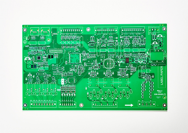
With over 30 years of experience in the industry, this seasoned manufacturer of Printed Circuit Boards (PCBs) is setting a new standard for excellence. Specializing in the production of high-quality Micro Via PCBs, the company is committed to providing state-of-the-art PCB products with precision and efficiency.
The company, located in China, has established itself as a leading manufacturer, supplier, and factory of PCBs with its advanced technology and cutting-edge equipment. Their dedication to quality and innovation has made them a trusted partner for businesses seeking reliable PCB solutions.
The Micro Via technology employed by the company enables the creation of PCBs with smaller and more precise vias, essential for high-density applications and complex designs. These Micro Via PCBs have a smaller diameter than traditional vias, resulting in increased routing space and higher connection density. With the ability to offer better signal integrity, lower signal loss, and reduced cross-talk, their Micro Via PCBs are designed to exceed performance expectations.
In addition to their technological advancements, the company's engineering team is dedicated to providing custom solutions tailored to specific requirements. They offer design services and can produce Micro Via PCBs with a variety of materials, finishes, and specifications to meet the unique needs of their clients.
Furthermore, the company's commitment to quality sets them apart from other PCB manufacturers. Their thorough inspection process throughout the PCB production process ensures that only high-quality PCB products are delivered to their customers. Whether it's PCB designing, assembly, or 3D PCB printing, the company maintains a keen focus on quality to meet the evolving needs of the electronics industry.
The revolutionary Micro Via PCBs offered by the company boast unmatched performance and compact design. These incredibly small, ultra-thin holes provide greater flexibility in routing and interconnecting components within a limited space. With state-of-the-art technology and the highest quality materials, the company ensures durability and reliability in their Micro Via PCBs.
The unique design of their Micro Via PCBs allows for enhanced signal integrity, making them perfect for high-frequency applications. With reduced signal loss and improved impedance control, their PCBs offer optimal performance even in the most complex designs. Additionally, the Micro Via PCBs offer excellent thermal management capabilities, effectively dissipating heat and preventing overheating issues, making them ideal for power-hungry applications.
Customer testimonials further solidify the company's reputation for excellence. Satisfied customers have emphasized the precision and reliability of the micro vias, along with the cost-effectiveness and exceptional performance of the PCB products. The company's commitment to exceeding customer expectations is evident through the positive feedback they have received.
In conclusion, this leading Micro Via PCB manufacturer in China is dedicated to delivering cutting-edge solutions that meet the evolving needs of the electronics industry. Their Micro Via PCBs are the ideal choice for projects requiring high-performance and space-saving designs. With a focus on quality, precision, and customer satisfaction, the company continues to set the standard for excellence in the PCB manufacturing industry.
For businesses seeking a reliable micro via PCB manufacturer, supplier, and factory in China, this company stands out as the top choice. With a track record of delivering high-quality PCB products with state-of-the-art technology and advanced equipment, the company is well-equipped to meet the diverse needs of their clients.
Contact the company today to learn more about their Micro Via PCBs and how they can exceed your expectations. In a rapidly evolving industry, this manufacturer remains at the forefront of innovation, delivering unmatched quality and precision in their PCB products.
Company News & Blog
Fast PCB Turnaround Time: Quick Solutions for Timely Printed Circuit Board Production
Fast PCB Turnaround: Transforming Electronics Manufacturing with Swift DeliveryIn today's rapidly evolving technology landscape, businesses are constantly pushing the boundaries of innovation, bringing groundbreaking products and solutions to the market. Among the key components crucial to successfully bringing these innovations to fruition is the Printed Circuit Board (PCB). PCBs serve as the backbone of electronic devices, allowing for the seamless integration of various electronic components. As the demand for faster turnaround times continues to grow, one company has emerged as a leading player in the fast PCB turnaround space, revolutionizing electronics manufacturing – we will refer to it as Company X.Established in (year), Company X has been at the forefront of providing swift PCB turnaround solutions to businesses across industries. With a steadfast commitment to quality, reliability, and customer satisfaction, they have set themselves apart from their competitors. This article will delve into the innovative approaches employed by Company X and explore the impact it has had on the electronics manufacturing industry.One of the key drivers behind Company X's success is their state-of-the-art manufacturing facilities equipped with the latest advanced machinery and technologies. By leveraging cutting-edge equipment, they have significantly reduced production time while maintaining the highest standards of quality. Their facilities utilize automated processes and robotic systems, enabling efficiency and precision at every stage of PCB production. These modern advancements contribute to faster turnaround times, ensuring that customers receive their PCBs promptly, even in critical time-sensitive projects.Apart from their advanced manufacturing capabilities, Company X understands the importance of a streamlined and efficient production workflow. They have implemented agile methodologies, ensuring optimized resource allocation and seamless collaboration across teams. By meticulously analyzing each step of the production process, they have identified areas where improvements can be made. These improvements have not only resulted in faster PCB turnaround but have also increased the overall productivity and cost-effectiveness of their operations.Moreover, Company X places great emphasis on their dedicated team of skilled professionals who are experts in PCB design and production. These professionals have been meticulously selected, boasting extensive experience and expertise in their respective fields. From design engineers to quality control specialists, their team works collaboratively, ensuring that each PCB is thoroughly reviewed and undergoes stringent quality checks before it reaches the customer. This attention to detail guarantees that customers receive PCBs of superior quality, leading to enhanced product performance and reliability.In addition to their cutting-edge facilities and talented workforce, Company X has also invested heavily in establishing strong relationships with their suppliers. They have forged strategic partnerships with trusted manufacturers of component parts, allowing them to procure materials on-demand and at competitive prices. This proactive approach to supply chain management ensures that there are no delays or bottlenecks in the production process. Their robust supplier network, coupled with agile inventory management, is instrumental in achieving fast PCB turnaround times.Furthermore, Company X understands that every customer is unique and has different project requirements. To cater to these varying needs, they offer a range of personalized services. From quick-turn prototypes to large-scale production orders, they have the flexibility to accommodate projects of any scale. Customers also have access to a dedicated support team, ready to address any queries or concerns throughout the entire production process. This commitment to exceptional customer service has earned Company X a reputation for reliability and client satisfaction.As the electronics manufacturing industry continues to evolve, the demand for fast PCB turnaround is only expected to increase. Company X has been at the forefront of meeting these demands and providing reliable and efficient solutions. Through their cutting-edge facilities, streamlined workflows, talented professionals, and personalized services, they have revolutionized the electronics manufacturing landscape. With their continued commitment to excellence, Company X is well-positioned to further enhance their position as a leader in fast PCB turnaround, driving innovation and enabling businesses to bring their ideas to life.
Fast PCB Manufacturing Supplier in China - Top Factory and Manufacturer
In exciting news for the tech industry, a China-based PCB manufacturing company is making waves with its lightning-fast turnaround times and top-quality products. With over 30 years of experience in the industry, this company has established itself as a leading player in the fast PCB manufacturing space.The company, which we will refer to as "Omni PCB" for the purpose of this article, specializes in producing high-quality PCBs for a wide range of industries and applications, including automotive, telecommunications, medical, and more. Whether it's a prototype or high volume production, Omni PCB's state-of-the-art facilities and experienced team enable them to offer fast turnaround times without sacrificing quality.At the heart of Omni PCB's operations is a commitment to delivering exceptional customer service and top-quality products. They understand the importance of having PCBs manufactured quickly and efficiently, which is why they offer a wide range of turnaround times to suit specific needs. Whether clients need their PCBs in a few hours or a few days, Omni PCB has them covered.But it's not just speed that sets Omni PCB apart - it's their unwavering commitment to quality. The company's attention to quality is what differentiates them from other PCB assembly companies. Every PCB product is inspected throughout the production process, whether it's PCB designing, assembly, or 3D PCB printing, to ensure that only high-quality products are delivered to clients.In addition to their fast PCB manufacturing services, Omni PCB also offers a range of other services, including PCB design, assembly, and testing. Their cutting-edge technology and state-of-the-art facility enable them to produce printed circuit boards at lightning-fast speeds without sacrificing quality. This, combined with their exceptional customer service and competitive pricing, makes them a sought-after partner for companies looking to bring their PCB projects to life.Customer testimonials speak volumes about Omni PCB's reputation in the industry. Ms. Carlen Shu, who recently tried out their fast PCB manufacturing service, was blown away by the speed and quality of their work. From submitting her design file to receiving the finished boards, the entire process took only a few days. The boards themselves were flawless with no mistakes or imperfections. Ms. Angela Her echoed similar sentiments, emphasizing the lightning-fast turnaround time and top-notch quality of Omni PCB's products.With their stellar track record and a growing list of satisfied clients, Omni PCB is poised to further solidify its position as a top player in the fast PCB manufacturing space. Their combination of speed, quality, and exceptional customer service makes them a standout choice for companies looking for reliable PCB manufacturing partners.As technology continues to advance at a rapid pace, the demand for fast and reliable PCB manufacturing services will only continue to grow. Companies like Omni PCB, with their focus on quality, efficiency, and customer satisfaction, are well positioned to meet this growing demand and carve out a lasting legacy in the industry.In conclusion, Omni PCB's commitment to delivering high-quality PCB products in record time, combined with their unwavering focus on customer satisfaction, makes them a force to be reckoned with in the fast PCB manufacturing space. As the tech industry continues to evolve, companies like Omni PCB will play a crucial role in bringing cutting-edge technologies to life, driving innovation, and pushing the boundaries of what's possible in the world of PCB manufacturing.
Leading Industry Experts Share Tips on Finding a Reliable 10 Layer PCB Manufacturer
[Company Name], a Leading 10 Layer PCB Manufacturer, Strengthens Position in the Market with Expanded Offerings and Cutting-Edge Technology[CITY], [DATE] - [Company Name], a renowned 10 Layer PCB manufacturer, has recently announced its plans to further solidify its position as an industry leader through the introduction of advanced technologies and expanded product offerings.At the forefront of the electronic manufacturing industry, [Company Name] has built a reputation for delivering high-quality and reliable PCB solutions. With an extensive range of capabilities, the company has been catering to the diverse needs of customers across various sectors, including telecommunications, automotive, industrial, and consumer electronics.One of the key factors contributing to [Company Name]'s success is its commitment to staying ahead of the technological curve. By investing in state-of-the-art equipment and continuously upgrading its manufacturing processes, the company ensures that it can meet the evolving demands of its customers.With the latest introduction of cutting-edge technology, [Company Name] now offers even more advanced PCB solutions to its clients. The expanded capabilities include enhanced signal integrity, multi-layer impedance control, high-frequency PCBs, and fine-pitch BGA routing. These improvements enable [Company Name] to provide its customers with efficient and reliable PCBs that meet the stringent requirements of modern electronic devices.In addition to technological advancements, [Company Name] has also expanded its product portfolio. By offering a wider variety of PCB types and materials, the company can cater to an even broader range of customer needs.Moreover, [Company Name] has developed a streamlined and efficient production process, ensuring high-quality deliverables and reduced lead times. By closely adhering to industry standards and employing rigorous quality control measures, the company has garnered a reputation for delivering PCBs that consistently meet or exceed customer expectations.Going forward, [Company Name] aims to further enhance its production capabilities through ongoing research and development initiatives. By staying at the forefront of emerging technologies, the company will continue to provide innovative and reliable PCB solutions to its customers."We are excited about the additional offerings and improved capabilities that we are bringing to the table," said [Company Name]'s CEO. "With the ever-evolving demands of the electronic industry, it is crucial for us to stay ahead and offer cutting-edge solutions that enable our customers to bring their products to market faster and with greater precision."[Company Name]'s commitment to customer satisfaction and continuous improvement has garnered it a loyal customer base, including renowned global electronics manufacturers. By consistently delivering superior PCB solutions, the company has established itself as a trusted and preferred partner for customers seeking high-quality electronic components.In conclusion, [Company Name], a leading 10 Layer PCB manufacturer, is bolstering its position in the industry by introducing advanced technologies and expanding its product offerings. With a commitment to staying ahead of the technological curve, the company aims to provide its customers with efficient and reliable PCB solutions that meet the evolving demands of the electronic industry.About [Company Name]: [Company Name] is a renowned 10 Layer PCB manufacturer that specializes in delivering high-quality and reliable PCB solutions. With state-of-the-art equipment and a commitment to technological advancements, the company caters to diverse customer needs across various sectors. Through streamlined production processes and rigorous quality control measures, [Company Name] ensures superior deliverables and customer satisfaction.
Unveiling the Latest Breakthrough: Harnessing the Power of FR4 Tg150 Technology
Innovative PCB Material Sets New Standards for Electronics IndustryWith a mission to constantly push the boundaries of technological advancements, a leading company in the electronics industry has recently introduced a groundbreaking PCB material known as FR4 TG150. Demonstrating a commitment to quality and innovation, this remarkable product is set to revolutionize the way electronic devices are designed and manufactured.The FR4 TG150, a cutting-edge PCB material, addresses the escalating demands of modern electronics. This high-performance material offers superior reliability, increased efficiency, and enhanced durability, making it highly sought after by engineers and manufacturers alike. The material's unique properties make it particularly well-suited for use in various applications, ranging from consumer electronics to industrial machinery.One of the key features that sets FR4 TG150 apart from traditional PCB materials is its exceptional thermal stability. By ensuring excellent heat resistance, this innovative material enables electronic devices to function optimally in the most demanding environments. With the rapid growth of technology, devices often face challenging conditions such as high temperatures or fluctuating thermal cycles. FR4 TG150 mitigates these concerns, making it an ideal choice for mission-critical applications.Furthermore, the FR4 TG150 also offers excellent mechanical strength and insulation properties. This enables it to withstand physical stress, reducing the risk of damage or failure during operation. By providing a high degree of reliability, the material proves itself as a formidable solution for industries where robustness and long-term functionality are paramount.In terms of electrical performance, FR4 TG150 excels in delivering superior signal integrity. Its low electrical loss allows for faster signal propagation and reduced signal distortions. This is particularly advantageous for high-speed digital circuits found in modern electronic devices. By minimizing signal degradation, the material ensures a higher level of accuracy and functionality, ultimately enhancing the overall user experience.The inherent versatility of FR4 TG150 makes it an ideal choice for various electronic applications. From smartphones and tablets to automotive electronics and aerospace systems, the material's adaptability meets the diverse needs of different industries. This enables engineers and designers to explore new possibilities, enabling the development of innovative and cutting-edge products.The introduction of FR4 TG150 heralds a new era in the electronics industry, propelling it towards greater heights. Industry experts are touting this revolutionary material as a game-changer, setting new standards for PCB manufacturing and design. With its exceptional thermal stability, mechanical strength, insulation properties, and electrical performance, FR4 TG150 is poised to redefine the benchmark for future electronic devices.As a leading company dedicated to providing comprehensive solutions for the electronics industry, the manufacturer of FR4 TG150 reaffirms its commitment to innovation and quality. Through relentless research and development efforts, they aim to empower engineers and manufacturers with groundbreaking solutions that meet the evolving demands of the digital age.In conclusion, FR4 TG150 represents an extraordinary advancement in PCB materials. Its exceptional properties and versatility make it a game-changer in the electronics industry. As this innovative material gains traction, it is expected to transform the way electronic devices are designed, manufactured, and experienced. With a company at the forefront of this technological revolution, the future of electronics looks promising, ushering in a new era of excellence.
China PCB and PCBA Manufacturer, Supplier, and Factory - High-Quality Products at Competitive Prices" Change to: "High-Quality PCB and PCBA Manufacturer, Supplier, and Factory - Competitive Prices Guaranteed
Omni PCB: Your Trusted Partner for High-Quality PCB and PCBA ProductsWith an experience of over 30 years old, Omni PCB is a seasoned manufacturer of high-quality Printed Circuit Board (PCB) and Printed Circuit Board Assembly (PCBA) products. With a state-of-the-art facility and refined processes, Omni PCB is dedicated to providing top-notch PCB components for various electronic devices.The company's commitment to quality and timely delivery sets it apart in the industry. In addition to ensuring that PCBs are delivered on time, Omni PCB places a strong emphasis on quality control throughout the production process, from design to assembly and 3D printing. This dedication to quality ensures that only the highest quality PCBs and PCBA components are delivered to customers.Omni PCB specializes in producing a wide range of PCB components, available in various sizes and materials including FR4, Aluminum, and Rogers. Additionally, the company offers flexible and rigid-flex PCB solutions to meet specific customer needs. The PCBA components are assembled using the latest Surface Mount Technology (SMT) and Dual In-line Package (DIP) technologies, ensuring efficient manufacturing and consistent product quality.The company's team of highly skilled engineers, designers, and technicians work together to ensure that every product meets the highest standards of quality and reliability. Whether it's a standard PCB or a custom-designed solution, Omni PCB is dedicated to providing products that meet or exceed customer expectations.Customer testimonials highlight the company's dedication to innovation and their ability to provide superior tools that meet high industry standards. Ms. Carlen Shu, a satisfied customer, praises the company's top-notch products and reliable solutions for electronic design and manufacturing needs. She highlights the precision and accuracy of the PCBs, as well as the quality materials and functionality of the PCBA components. Ms. Angela Her emphasizes the importance of quality and reliability in PCB and PCBA components and recommends choosing products from specialized and trustworthy manufacturers.In addition to offering standard PCB and PCBA products, Omni PCB provides custom design and manufacturing services to meet specific requirements. The company's experienced engineering team works closely with customers to develop customized solutions that deliver the performance needed for their applications.The company's expertise in producing high-quality PCB and PCBA products extends to a variety of application needs, from consumer electronics to industrial control systems. With a commitment to quality and customer satisfaction, Omni PCB is the ideal choice for customers looking for reliable and high-quality PCB and PCBA products.Omni PCB also offers a full turnkey solution for electronic assembly needs, from design and prototyping to production and testing. The company uses only the highest quality components and employs rigorous quality control processes to ensure that every circuit board meets strict industry standards.For customers in search of a reliable PCB and PCBA manufacturer, supplier, or factory in China, Omni PCB stands out as a top choice. With top-notch services, the company ensures quality products and timely delivery. Customers can trust Omni PCB to deliver the best products and service in the industry.In conclusion, Omni PCB is a trusted partner for high-quality PCB and PCBA products. With a focus on quality, innovation, and customer satisfaction, the company is committed to providing top-notch solutions for electronic design and manufacturing needs. Contact Omni PCB today to learn more about their products and services.In summary, Omni PCB is a leading manufacturer and supplier of high-quality PCB and PCBA components for various electronic devices. The company's commitment to quality and customer satisfaction, combined with its state-of-the-art facility and advanced production equipment, sets it apart in the industry. Whether it's standard PCB and PCBA products or custom-designed solutions, customers can trust Omni PCB to deliver top-notch products and reliable service. Contact Omni PCB today to learn more about their high-quality PCB and PCBA products and services.
In-House Circuit Card Assembly Capabilities at Battelle
Building and Testing Circuit Card Assembly BoardsCircuit Card Assembly Testing is an essential requirement for ensuring the quality and reliability of electronic devices. From consumer electronics to industrial controls, virtually all electronic devices rely on robust and reliable circuit boards to function properly. A Circuit Card Assembly (CCA) Board is a key component in any electronic device, and it is essential that the assembly process and testing procedures are done correctly for optimal performance.A Circuit Card Assembly Board is a complex and intricate system that requires precision manufacturing techniques to build, assemble, and test. A CCA Board is composed of several electronic components, including resistors, capacitors, diodes, transistors, and integrated circuits, among other things. Each component plays a vital role in the overall functionality and reliability of the board.The Build ProcessBuilding a Circuit Card Assembly Board requires a set of standard procedures and significant technical expertise. The assembly process starts with the design of the board and identifying the electronic components that will be required to build the board. The board must be optimized with a design that meets the necessary electrical, thermal, and mechanical requirements.Once the design is finalized, the schematic design is converted into a layout that can be used for manufacturing. The layout of the board is used to create a stencil that is used to place the electronic components precisely. The stencil ensures that each component is placed correctly to avoid any shorts or misplacing of electronic components.Once the board's stencil is created, the board is manufactured by carefully placing each electronic component on the board, using automated machines and careful manual labor. The components are then assembled using solder paste that allows the components to adhere to the board and provides electrical contact.Testing the Circuit Card Assembly BoardWith the board successfully assembled, the next and most crucial step is testing the Circuit Card Assembly Board. Testing ensures that the board functions correctly, meets the specifications, and is free from defects.The testing process involves several steps, and it is highly dependent on the type of board and its intended use. The common types of testing include:- Visual Inspection: A Visual Inspection is performed to ensure that there are no visible defects, including bent pins, missing components, or shorts.- Functional testing: Function testing is carried out to verify that the board functions correctly. It involves applying power to the board and checking that each electronic component is working correctly. Functional testing can be automated or done manually, depending on the complexity of the board.- Environmental testing: Environmental testing simulates the operating environment of the board and is done to ensure that the board can operate correctly in harsh conditions. Environmental testing includes temperature cycling, vibration testing, and shock testing.- Burn-in Testing: Burn-in testing is carried out to verify the reliability of the board. The Board is subjected to long term stress testing to identify any defects that may not be noticeable during initial testing.In-house CapabilityManufacturing and testing Circuit Card Assembly Boards require a high level of technical expertise, experience, and sophisticated equipment. Circuit Card Assembly Board builds or circuit card assemblies (CCA) are a crucial in-house capability that any electronic device manufacturer should possess. Battelle (remove the brand name) has invested heavily in Equipment, personnel, and training to ensure that they have the capability to build and test CCA boards.In conclusion, Circuit Card Assembly Testing is a critical aspect of ensuring the quality and reliability of electronic devices. Building and Testing Circuit Card Assembly Boards require the right equipment, expertise, and a highly trained workforce. Circuit Card Assembly Board builds or circuit card assemblies (CCA) are a crucial in-house capability that any electronic device manufacturer should possess. If you're looking for a reliable and experienced company to build and manufacture CCA boards, look no further than Battelle's Electronics and Manufacturing Services Division.
High-Quality PCBs Available Online from Leading Manufacturers in China - Competitive Prices
In today's rapidly evolving technological landscape, the demand for high-quality printed circuit boards (PCBs) has never been higher. As businesses and individuals alike continue to push the boundaries of innovation in electronics and manufacturing, the need for reliable and efficient PCB suppliers has become increasingly critical. Recognizing this demand, Omni PCB, a seasoned manufacturer with over 30 years of experience, has unveiled its cutting-edge PCB online platform - a game-changing solution that promises to revolutionize the way PCBs are manufactured and procured.Omni PCB's commitment to excellence is evident in its state-of-the-art PCB products. With an unwavering focus on quality and a dedication to delivering top-notch PCBs in the shortest possible time, Omni PCB has established itself as a trusted and reliable supplier in the industry. The company's refined processes and strict quality control measures ensure that every PCB produced is inspected throughout the production process, from designing to assembly and 3D printing, to guarantee exceptional performance and reliability.Building on this strong foundation, Omni PCB has introduced its groundbreaking PCB online platform - an innovative solution designed to streamline the PCB procurement process, eliminate manual paperwork, and reduce communication cycles. With a comprehensive range of customization options available, users can easily tailor their PCBs to meet their exact requirements, whether it's a simple single-layer board or a complex multilayer design. The user-friendly interface allows for swift uploading of designs, selection of specifications, and seamless order placement directly from the comfort of a computer, ultimately saving valuable time and resources and leading to faster product turnaround.What sets Omni PCB's online platform apart is its ability to provide real-time quotations and instant access to pricing information. By leveraging its extensive network of top-tier PCB manufacturers, the company guarantees competitive pricing and exceptional lead times, making it quick and easy for engineers, designers, and businesses to order custom PCBs. Furthermore, the platform offers a wide range of materials, thicknesses, finishes, and other specifications tailored to specific project requirements, ensuring optimal performance and customization flexibility.Customer satisfaction is at the heart of Omni PCB's mission, and the company's commitment to delivering a convenient and reliable experience is reflected in the glowing reviews from satisfied customers. With a wide selection of PCBs to choose from, a smooth and hassle-free ordering process, impressive turnaround times, and excellent quality, customers have expressed their high satisfaction with the PCBs they have ordered online. These testimonials serve as a testament to Omni PCB's unwavering dedication to providing top-notch quality and unmatched convenience.As the world continues to embrace the future of PCB manufacturing, Omni PCB's innovative online platform is primed to play a pivotal role in shaping the industry's landscape. Whether one is a hobbyist, a startup, or an established company, the platform is designed to cater to a wide range of needs and budgets, reaffirming Omni PCB's position as China's premier supplier for wholesale, export, and OEM options.In conclusion, Omni PCB's introduction of its revolutionary PCB online platform marks a significant milestone in the electronics manufacturing industry. With an unwavering commitment to quality, unmatched convenience, and exceptional customer service, the company remains at the forefront of delivering high-quality PCBs at competitive prices. As the industry continues to evolve, Omni PCB is poised to lead the way in providing innovative solutions that meet the ever-increasing demand for advanced and efficient electronics. Experience the future of PCB procurement with Omni PCB's innovative online platform and unlock a world of seamless PCB manufacturing.
In today's digital world, the printed circuit board (PCB) is a crucial component in the operation of electronic gadgets of all types. This essential piece is responsible for the electrical connections between components, enabling the flow of information and power within a device. One of the most widely used types of PCBs is the flexible printed circuit board, or FPC.FPCs are used in an array of applications, ranging from simple consumer electronics to complex medical equipment. These PCBs offer a range of benefits, including high precision, improved form factor, and increased reliability. However, the manufacturing of FPCs can be a complex process, requiring advanced methods and technologies to achieve high-quality products.This is where companies like AIRTECH Global come in. Utilizing their unique multilayer manufacturing technology, AIRTECH has been able to help their customers increase their lamination area performance. This means that they provide assistance to their clients in creating high-quality FPCs that are reliable, efficient, and cost-effective.One of the primary benefits of utilizing AIRTECH's products is the ability to lower production costs. By streamlining the manufacturing process and using advanced technologies, they can create FPCs with higher yields, better precision, and fewer errors. This, in turn, leads to a decrease in the production costs associated with FPCs, making them more accessible for consumers and businesses alike.Another benefit of using AIRTECH's products is the improved performance of FPCs. Their multilayer manufacturing technology enhances the electrical and thermal properties of the FPCs, making them more reliable and efficient. This means that the devices that incorporate these FPCs will perform better and last longer, adding to the overall value of the product.In addition to FPCs, AIRTECH also provides lamination assist products for rigid-flex boards and high layer count/HDI PCB/PWB boards. This means that they can assist their clients in creating a wide range of PCBs that meet their specific needs and requirements.Overall, AIRTECH's unique multilayer manufacturing technology is revolutionizing the world of FPCs and other PCBs. By lowering production costs, improving performance, and providing a range of products and services, they are helping businesses of all types create high-quality electronic devices that are reliable and efficient. As the demand for advanced electronics continues to grow, companies like AIRTECH will continue to play a crucial role in the industry, providing the products and services that make it all possible.
China Manufacturer & Supplier of Double Sided Copper Clad Boards - Factory Price
Title: Leading Manufacturer in China Offers Top-Quality Double Sided Copper Clad BoardsIn the fast-paced world of electronics, having access to top-quality Double Sided Copper Clad Boards is essential for designers and hobbyists alike. Fortunately, there is a reliable manufacturer in China that offers a range of high-performance circuit boards designed to meet the highest industry standards.With over 30 years of experience, this leading manufacturer, known for their commitment to quality and reliability, is the go-to supplier for Double Sided Copper Clad Boards. Their state-of-the-art manufacturing processes and attention to detail ensure that every board meets exact specifications and requirements.Their Double Sided Copper Clad Boards are made with the highest quality materials, providing excellent solderability and conductivity. These boards are perfect for a wide range of electronic applications, from professional electronics design to DIY projects. Whether you are working on automotive, aerospace, medical, or telecommunications applications, their boards are designed to meet the most demanding requirements.The company prides itself on offering superior customer service, with a dedicated team available to answer any questions and provide support throughout the ordering process. Whether you are a seasoned professional or a hobbyist, you can trust this manufacturer to deliver superior quality and performance every time.Double Sided Copper Clad Boards are a must-have for creating effective and efficient circuit boards. They offer a broad range of benefits, including high thermal and electrical conductivity, as well as resistance to corrosion. With double-sided designs, these boards make it easier to transfer signals from one side of the board to the other, and their durability and strength are unmatched.These boards are compatible with a wide range of soldering techniques, making them ideal for use in both manual and automated assembly processes. Their versatility and unrivaled performance make them the perfect choice for electronic circuit board needs.The company's commitment to quality and reliability is further evidenced by the glowing reviews from satisfied customers. One customer, Ms. Carlen Shu, expressed that the Double Sided Copper Clad Board is an essential tool for anyone working with electronics, praising its high-quality copper and double-sided design. Another customer, Ms. Angela Her, highlighted the board's easy soldering and signal integrity, making it the perfect investment for anyone looking to work with electronics.In addition to their exceptional product quality, the company also places a strong emphasis on timely delivery. They understand the importance of delivering PCB products as agreed upon and as early as possible, supporting their clients, employees’ R&D work, and prototyping needs.The manufacturer's refined processes and attention to quality set them apart from other PCB assembly companies. Their PCB products are inspected throughout the production process, from design to assembly, to ensure only high-quality products are delivered.In conclusion, for anyone looking for a reliable manufacturer, supplier, or factory of Double Sided Copper Clad Boards, the search ends in China. With top-quality boards designed to meet the highest industry standards and competitively priced, this leading manufacturer is the best choice for any project. Contact them today to experience superior quality and performance in every board.
Top Low Volume PCB Manufacturer and Supplier - Factory Direct Prices!
Omni PCB, a seasoned manufacturer of Printed Circuit Boards, has been providing top-quality PCB products for over 30 years. With a strong focus on delivering high-quality PCBs in the shortest possible time, Omni PCB has earned a reputation as a reliable and trustworthy supplier in the industry.As the demand for low volume PCBs continues to grow, finding a reliable manufacturer has become increasingly important for businesses and tech enthusiasts alike. The search for a low volume PCB manufacturer can be challenging, but Omni PCB is here to provide a solution. The China-based company is a leading supplier of high-quality PCBs, delivering fast turnaround times at competitive prices. With a focus on producing PCBs in small to medium volume quantities, Omni PCB specializes in creating custom solutions tailored to the exact specifications of their customers. Whether it's a simple 2-layer PCB or a more complex multi-layer PCB, the team of experts at Omni PCB can bring any project to life.One of the key factors that sets Omni PCB apart from other suppliers is their commitment to using high-quality components in PCB production. The company takes great care in sourcing the best materials to ensure that their PCBs meet the highest industry standards. With state-of-the-art facilities and advanced manufacturing equipment, Omni PCB is able to produce PCBs with superior quality and accuracy.Quality is a top priority at Omni PCB, with stringent quality control measures in place at every stage of production to ensure that each PCB meets the exact specifications of the customer. Their attention to detail and commitment to delivering high-quality, reliable, and cost-effective PCBs has earned them a positive reputation in the industry.For tech enthusiasts with unique project ideas, Omni PCB offers a range of customized services to meet specific project requirements. The company's team of skilled engineers works closely with customers to ensure that they receive the best possible product. Whether it's five or five hundred PCBs, Omni PCB has the resources and expertise to turn any concept into a reality.The company's dedication to quality and customer satisfaction is reflected in the positive feedback from their clients. Ms. carlen shu, a satisfied customer, shared her experience with Omni PCB, praising their quick and efficient service, affordable pricing, and attention to detail. Another customer, Ms. Angela Her, highlighted the company's ability to produce high-quality and precision-made PCBs with quick turnaround times, making them a top-rated provider in the industry.In addition to their outstanding customer reviews, Omni PCB's commitment to innovation is also evident in their state-of-the-art equipment and years of experience, allowing them to meticulously produce PCBs with precision and accuracy that meet any industry standard.As the demand for low volume PCBs continues to grow, Omni PCB stands out as a reliable and trustworthy OEM supplier in China. The company's dedication to delivering exceptional products and services, combined with their expertise in producing high-quality PCBs, makes them an ideal choice for businesses and individuals in need of low volume PCB manufacturing.Whether it's for prototyping, R&D work, or small batch runs, Omni PCB offers competitive pricing without compromising on quality. With their focus on delivering high-quality, reliable, and cost-effective PCBs, Omni PCB is the go-to solution for all low volume PCB manufacturing needs.In conclusion, Omni PCB's dedication to quality, innovation, and customer satisfaction makes them the top choice for businesses and tech enthusiasts in need of a reliable and trustworthy low volume PCB manufacturer. With their state-of-the-art facilities, advanced manufacturing equipment, and years of experience, Omni PCB is well-equipped to meet the needs of any project, big or small. Contact Omni PCB today to experience the difference for yourself.