
Top Trend: Exploring the Potential of Copper Base PCB for Advanced Applications
By:admin
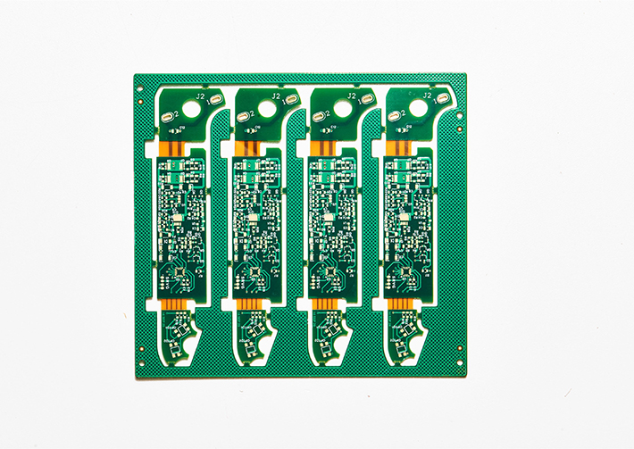
Copper Base PCBs are revolutionizing the electronics industry with their exceptional thermal conductivity and durability. One such company leading the charge is [Company Name], specializing in the manufacturing and development of superior Copper Base PCB solutions. With a vision to revolutionize electronic devices, [Company Name] has established itself as a leading provider of innovative and high-quality Copper Base PCBs. This article will delve into their journey, products, and the impact they are making in the industry.
[Company Overview]
Established in [Year], [Company Name] has been at the forefront of developing cutting-edge Copper Base PCBs. With a team of experienced engineers and a state-of-the-art manufacturing facility, the company has successfully carved a niche for itself in the highly competitive market. Their commitment to quality, innovation, and customer satisfaction sets them apart.
[Products and Solutions]
[Company Name] offers a wide range of Copper Base PCBs tailored to suit various industry and application requirements. Their in-house research and development team ensures that each product is designed meticulously to deliver optimal performance. Here are some prominent offerings by [Company Name]:
1. Copper Base Single-sided PCB: These PCBs are widely used in applications requiring efficient heat dissipation. [Company Name] ensures that their single-sided Copper Base PCBs provide excellent thermal conductivity and electrical insulation for optimal performance.
2. Copper Base Double-sided PCB: Ideal for applications needing higher power requirements, these PCBs comprise a double-sided copper layer for enhanced thermal management. The design and manufacturing expertise of [Company Name] ensures exceptional performance and reliability.
3. Copper Base Multilayer PCB: Complex electronic devices demand multilayer PCBs, and [Company Name] meets this requirement with their Copper Base Multilayer PCBs. These products provide excellent thermal conductivity while allowing for multiple layers of circuitry.
4. Copper Base High-Frequency PCB: With the increasing demand for high-frequency applications, [Company Name] provides Copper Base PCBs that are optimized for exceptional signal integrity and low loss. These specialized PCBs ensure efficient power distribution and enhanced performance.
5. Customized Copper Base PCBs: [Company Name] understands that each customer may have unique requirements. Therefore, they offer customized solutions to cater to specific needs. Their skilled engineers work closely with clients to deliver tailor-made Copper Base PCBs with precise specifications.
[Industry Impact and Future Prospects]
The introduction of Copper Base PCBs has significantly impacted the electronics industry. With their superior thermal conductivity and durability properties, Copper Base PCBs enable electronic devices to operate more efficiently and reliably. They are particularly crucial in high-power applications and can withstand extreme temperatures.
[Company Name] has been instrumental in pushing the boundaries of Copper Base PCB technology. Their commitment to quality and continuous innovation has earned them a commendable reputation in the market. They strive to keep pace with emerging trends and technologies to deliver advanced and reliable solutions to their clients.
Furthermore, [Company Name] has also contributed to a more sustainable electronics industry. By ensuring efficient thermal management, Copper Base PCBs reduce energy consumption and extend the lifespan of electronic devices, thus minimizing electronic waste.
Looking ahead, [Company Name] aims to expand its global presence and explore new applications for Copper Base PCBs. They foresee further advancements in the field, such as improved integration with emerging technologies like IoT and 5G. With their dedication to excellence, [Company Name] is poised to play a pivotal role in shaping the future of Copper Base PCBs.
[Conclusion]
[Company Name] has made significant strides in the development and manufacturing of Copper Base PCBs. Their commitment to quality, innovation, and customer satisfaction has positioned them as industry leaders. With a robust product portfolio, including customized solutions, the company continues to revolutionize the electronics industry. As they forge ahead, [Company Name] aims to make a lasting impact while spearheading advancements in Copper Base PCB technology.
Company News & Blog
PCB Assembly Solderability Validation Tests Ensure High-Quality Standards
ATP's PCB Assembly Solderability Validation Tests: Ensuring the Highest Standards of QualityThe reliability and endurance of printed circuit board assemblies (PCBAs) are critical factors that determine their overall performance. Defective PCBs can disrupt entire systems and negatively impact product functionalities. That's why PCB assembly validation tests are vital in ensuring that the PCBAs meet the highest quality standards. ATP is a renowned company that specializes in delivering reliable and high-performance PCB assemblies. One of their crucial tests is the PCB Assembly Solderability Validation Test.PCB Assembly Solderability Validation TestThe solderability of a PCB refers to its ability to form a durable and strong bond with the intended components through the soldering process. Various factors can affect the performance of the solder joints, including oxidation, moisture, and contamination. PCB Assembly Solderability Validation Test is an essential test that aims to evaluate the soldering capability of the PCB. Additionally, this test confirms that the PCBs are free of contamination, oxidation, or any other factors that could hinder the formation of a strong bond.The Test ProcessThe PCB Assembly Solderability Validation Test process starts by identifying the critical components of the PCB assembly. The process evaluates the adhesion and compatibility of the components with the PCB by exposing them to environmental conditions that could potentially affect their performance. After evaluating the components, the PCB goes through a series of tests to confirm that the assembly process meets the industry standards.The test process involves using solder paste and reflow soldering to evaluate the quality of the PCBAs. The PCB is heated to a specific temperature, and the solder paste is applied to the board's surface. The solder forms a strong bond with the PCB, making it possible to attach various components to the PCB. The tests evaluate the solderability aspect of the PCB, which is an essential factor for the assembly's overall quality.Testing StandardsThe PCB Assembly Solderability Validation Test follows various industry standards, including the IPC J-STD-001, which outlines the requirements for the quality and reliability of soldered electrical and electronic assemblies. The test protocols ensure that all components are adequately and thoroughly inspected, including the electrical connections, surface mount components, and through-hole components. Additionally, this test confirms that the assemblies comply with the industry standards for surface finish, hole filling, and component alignment.Benefits of the PCB Assembly Solderability Validation TestThe PCB Assembly Solderability Validation Test ensures that the PCBs are free from defects that could compromise their performance. The test leads to a significant reduction in the risk of product failure and increases the overall reliability of the PCB assembly. Additionally, the test ensures that the PCBs meet the highest quality standards set by the industry, which is crucial in meeting the customer's expectations.ConclusionATP is committed to delivering high-quality PCB assemblies that meet the highest standards of quality and reliability. The PCB Assembly Solderability Validation Test is an essential part of the many reliability and endurance tests developed and performed by ATP to ensure strict compliance with the highest quality standards. The test ensures that the PCBs are free from defects that could potentially compromise their performance and overall reliability. By using the latest testing standards, ATP ensures the optimal quality of the PCB assemblies to meet the customer's expectations.
Pcb Prototype Service: A Guide to Efficient Prototyping Services
[Date][Headline][Subtitle][City], [State] - [Company Name], a leading provider in the electronics manufacturing industry, has recently introduced its newest service: PCB Prototype. This service aims to revolutionize the product development process by offering quick and reliable solutions for the manufacturing of printed circuit boards (PCBs).With the increasing demand for smaller, faster, and more complex electronic devices, the need for efficient and cost-effective PCB prototyping has become paramount. [Company Name] has recognized this market demand and has invested heavily in the development of its PCB Prototype Service to address these growing needs.One of the key features of [Company Name]'s PCB Prototype Service is its ability to provide a fast turnaround time. Traditional manufacturing processes often require weeks, if not months, to produce a functioning prototype. However, [Company Name] is promising its customers a significantly reduced lead time, ensuring that prototypes can be produced and delivered in a matter of days rather than weeks.The company achieves this fast turnaround time by streamlining its processes and utilizing state-of-the-art machinery. [Company Name] has heavily invested in advanced manufacturing equipment, including high-quality materials and cutting-edge software, to ensure the highest level of accuracy and efficiency in its PCB prototyping.Additionally, [Company Name]'s PCB Prototype Service offers unparalleled flexibility. Its manufacturing capabilities allow for a wide range of PCB designs, from single-sided to multi-layered boards. This versatility enables companies of all sizes and industries to benefit from [Company Name]'s PCB Prototype Service, regardless of their specific product requirements.Furthermore, [Company Name] understands that quality control is of utmost importance in the electronics manufacturing industry. To ensure that its customers receive only the highest quality prototypes, the company has implemented rigorous quality assurance procedures throughout its manufacturing process.In addition to fast turnaround times, flexibility, and quality control, [Company Name]'s PCB Prototype Service also boasts cost-effectiveness. By leveraging economies of scale and optimizing its manufacturing processes, the company is able to offer competitive pricing for its services without compromising on the quality of the end product.The introduction of [Company Name]'s PCB Prototype Service marks a significant milestone in the company's ongoing commitment to innovation and customer satisfaction. With this new service, [Company Name] is poised to become a leader in the PCB prototyping industry, catering to the needs of both small startups and established corporations alike.[Company Name] is confident that its PCB Prototype Service will enable its clients to accelerate their product development process, streamline operations, and bring their innovations to market faster than ever before. By offering a one-stop solution for PCB prototyping needs, [Company Name] aims to establish long-lasting partnerships with its clients and become their trusted go-to partner for all their electronics manufacturing requirements.As the demand for smaller, faster, and more advanced electronic devices continues to grow, [Company Name] remains committed to staying at the forefront of technology, providing innovative solutions, and meeting the evolving needs of its customers.For more information about [Company Name]'s PCB Prototype Service and other offerings, please visit [Company website]. About [Company Name]:[Company Name] is a leading electronics manufacturing company specializing in the production of high-quality printed circuit boards (PCBs) and electronic components. With a reputation for excellence and a commitment to customer satisfaction, [Company Name] has been serving a wide range of industries, including automotive, telecommunications, medical, and consumer electronics, for over [number] years. By combining advanced technology, state-of-the-art facilities, and a highly skilled team, [Company Name] continues to provide cutting-edge solutions for all electronics manufacturing needs.
High-Quality PCB Enclosure Manufacturer and Supplier in China - Wholesale Factory Direct Enclosures
Omni PCB, a trusted manufacturer, supplier, and factory based in China, has been providing high-quality Printed Circuit Boards (PCBs) for over 30 years. Their commitment to excellence has made them a leader in the industry, offering state-of-the-art PCB products with a focus on quality and timely delivery.When it comes to PCB enclosures, Omni PCB is the go-to choice for anyone looking for superior protection for their electronic projects. The company's PCB enclosures are designed to ensure the safety and security of printed circuit boards, even in the most demanding environments. Whether for DIY projects or industrial applications, Omni PCB offers a wide range of PCB enclosures in different sizes, materials, and designs to meet unique requirements and budget constraints.Omni PCB's PCB enclosures are crafted using only the highest-quality materials and advanced manufacturing techniques, ensuring consistent quality and performance. The company also offers custom design and manufacturing services to create PCB enclosures that perfectly match specific specifications and branding needs.One of the key features of Omni PCB's PCB enclosure is its robust structure, which provides maximum protection for PCBs while maintaining easy access for quick repairs or maintenance. This flexibility and durability make it the perfect solution for shielding PCBs from harmful elements such as dust, moisture, and other environmental factors.Additionally, the PCB enclosures are compact and lightweight, allowing seamless integration into tight spaces or cramped installations. The company offers various customization options, including shapes, sizes, colors, and mounting options, to meet project requirements. These features make it suitable for a wide range of industries, such as automotive, aerospace, medical, and more.Customers who have used Omni PCB's PCB enclosures have expressed high satisfaction with the product. They have praised the sturdy construction, clear cover for easy monitoring of circuit boards, ample space for wiring and components, and sleek, modern design. The PCB enclosure has been described as a reliable and attractive solution for protecting electronics, offering stability and excellent protection for PCBs.Omni PCB's attention to quality is what sets them apart from other PCB assembly companies. Their PCB products undergo thorough inspection throughout the production process, including PCB designing, assembly, and 3D PCB printing, to ensure that only high-quality products are delivered to customers.In addition to quality, timely delivery is another important factor for PCB suppliers, and Omni PCB is committed to ensuring that PCBs are delivered as agreed upon and as early as possible. This dedication to meeting delivery schedules has made them a trusted and reliable partner for customers' R&D work and prototyping needs.As a leading manufacturer in China, Omni PCB's dedication to quality and customer satisfaction has made them the ideal choice for anyone in need of premium PCB enclosures. Their extensive experience, commitment to excellence, and ability to deliver high-quality products in a timely manner set them apart in the industry.For anyone looking for a reliable and reputable PCB enclosure manufacturer, supplier, or factory in China, Omni PCB is the perfect choice. Contact them today to learn more about their wide range of PCB enclosures and how they can help build the next successful project.
Streamlining PCB Services for Hassle-free Solutions
Turnkey PCB Services Revolutionize the Electronics Manufacturing IndustryInnovation in the field of electronics manufacturing has taken another leap forward with the introduction of turnkey PCB services. These comprehensive solutions have transformed the industry by simplifying and streamlining the complex process of Printed Circuit Board (PCB) fabrication and assembly. By offering end-to-end support, turnkey PCB services have become increasingly popular among businesses looking to improve efficiency and reduce costs.Historically, the process of PCB manufacturing involved multiple stages and required involvement from different vendors, making it a cumbersome and time-consuming task. However, turnkey PCB services have changed the game by offering a one-stop solution for all PCB manufacturing needs. From design and prototyping to fabrication and assembly, a turnkey service provider takes care of the entire production process, ensuring a smooth and hassle-free experience for businesses.One key advantage of turnkey PCB services is the ease of collaboration during the design and prototyping phase. By working closely with the customer, the service provider can understand the unique requirements and specifications, and offer tailored solutions accordingly. This collaborative approach not only saves time but also minimizes the chances of errors, resulting in a more accurate and efficient PCB design.Moreover, turnkey PCB services offer a seamless transition from design to production. Once the prototype is approved, the service provider takes charge of the fabrication process, ensuring the highest quality standards are met. By leveraging advanced manufacturing technologies and techniques, turnkey services providers can deliver PCBs with increased precision and reliability, meeting the growing demands of the electronics industry.Another added benefit of turnkey PCB services is the consolidation of the supply chain. Traditionally, businesses had to deal with multiple vendors, resulting in challenges such as delays, miscommunication, and higher costs. However, turnkey PCB services eliminate these issues by managing all aspects of the supply chain, from sourcing components to quality control. By optimizing the procurement process and leveraging their industry expertise, turnkey service providers ensure a faster and more cost-effective production cycle.Furthermore, turnkey PCB services offer flexibility and scalability, catering to the unique needs of different businesses. Whether it's a small or large-scale production requirement, a turnkey service provider can efficiently handle the workload and meet deadlines. This scalability allows businesses to focus on their core competencies instead of worrying about the intricacies of PCB manufacturing, ultimately leading to improved productivity and profitability.Additionally, turnkey PCB services have become instrumental in reducing time-to-market for businesses. With the ever-increasing pace of technological advancements, companies need to bring their products to market quickly. Turnkey services providers streamline the manufacturing process, significantly reducing the time required for production. This accelerated time-to-market gives businesses a competitive edge, allowing them to seize opportunities and stay ahead in the fast-paced electronics industry.Overall, turnkey PCB services have revolutionized the electronics manufacturing industry by simplifying the complex process of PCB fabrication and assembly. With their end-to-end support, collaborative design approach, consolidated supply chain, flexibility, and scalability, these services have become a game-changer for businesses aiming to improve efficiency and reduce costs. By leveraging turnkey PCB services, companies can focus on innovation and product development, while leaving the intricacies of manufacturing in the hands of experts.
Key Factors to Consider When Choosing a Printed Circuit Board
Printed Circuit Board (PCB) is an essential component in almost every electronic device. It serves as the foundation for the electrical connections and mechanical support of various electronic components. Recently, a growing demand for PCBs has been observed due to the increasing usage of electronic devices in various industries such as consumer electronics, automotive, aerospace, and healthcare. This has led to a surge in competition among PCB manufacturers to produce high-quality and cost-effective solutions to meet the market demands.One of the leading companies in the PCB industry is {}. With years of experience and expertise in the field, {} has established itself as a reliable and innovative provider of PCB solutions. The company offers a wide range of PCB products, including single-sided, double-sided, and multi-layered PCBs, as well as flexible and rigid-flex PCBs.In addition to its diverse product offerings, {} is known for its state-of-the-art manufacturing facilities and advanced technologies that enable them to produce high-quality PCBs with precision and efficiency. The company's commitment to continuously investing in research and development has allowed them to stay ahead of the competition and offer cutting-edge PCB solutions to their clients.With a customer-centric approach, {} aims to provide personalized and reliable services to meet the unique requirements of each client. The company's team of skilled engineers and technicians work closely with clients to understand their needs and deliver tailored PCB solutions that meet or exceed their expectations.Furthermore, {} is dedicated to upholding the highest standards of quality and reliability in their products. The company adheres to stringent quality control measures throughout the manufacturing process to ensure that every PCB they produce meets the industry's standards and regulations.As part of its commitment to sustainability and environmental responsibility, {} also prioritizes eco-friendly manufacturing practices. The company strives to minimize its environmental footprint by implementing green initiatives and using sustainable materials in its manufacturing processes.In response to the growing demand for PCBs, {} has been expanding its production capacity and investing in new technology to meet the needs of its clients. The company's dedication to innovation and customer satisfaction has positioned it as a trusted partner for businesses across various industries, seeking high-quality PCB solutions.Looking ahead, {} is poised to further solidify its position as a market leader in the PCB industry by continuing to innovate and adapt to the evolving needs of the electronics market. With its unwavering commitment to excellence and customer satisfaction, the company is well-positioned to meet the increasing demand for PCBs and set new benchmarks in the industry.
Fast Turnaround PCB Services: Get Quick Manufacturing for Your Printed Circuit Boards
Quick Turn PCB, a leading provider of high-quality printed circuit board (PCB) solutions, has announced the launch of their new quick turn PCB service. This new service aims to provide customers with fast and efficient turnaround times for their PCB orders, meeting the increasing demand for rapid prototyping and production in the electronics industry.With over 15 years of experience in the PCB manufacturing industry, Quick Turn PCB has established a strong reputation for delivering reliable and cost-effective solutions to their clients. The company is equipped with state-of-the-art manufacturing facilities and a team of experienced engineers and technicians, allowing them to offer a wide range of PCB manufacturing services, including quick turn PCBs, multilayer PCBs, and prototype PCBs.The new quick turn PCB service will allow customers to expedite the production and delivery of their PCB orders, enabling them to bring their products to market faster. The service is designed to cater to the needs of businesses and individuals who require small to medium volume PCB production with quick turnaround times. Quick Turn PCB understands the importance of speed and agility in today's fast-paced electronics industry, and they are committed to helping their clients stay ahead of the competition."We are excited to introduce our new quick turn PCB service to meet the growing demand for rapid prototyping and production in the electronics industry," said a spokesperson for Quick Turn PCB. "With our advanced manufacturing capabilities and dedicated team, we are confident that we can provide our customers with the fast and efficient PCB solutions they need to bring their products to market quickly and effectively."In addition to their quick turn PCB service, Quick Turn PCB offers a range of value-added services to further support their clients' PCB needs. These services include design for manufacturability (DFM) analysis, PCB assembly, and testing, ensuring that customers receive comprehensive support throughout the entire PCB manufacturing process.With a commitment to quality, reliability, and customer satisfaction, Quick Turn PCB has established strong partnerships with clients from various industries, including aerospace, telecommunications, medical devices, and consumer electronics. The company's dedication to excellence and innovation has positioned them as a trusted partner for PCB manufacturing solutions."We take pride in delivering high-quality PCB solutions that meet the unique requirements of our customers," the spokesperson added. "Our new quick turn PCB service is a testament to our ongoing commitment to provide fast and reliable PCB manufacturing services that enable our clients to bring their innovative ideas to life."As the demand for quick turn PCB solutions continues to grow, Quick Turn PCB is well-positioned to meet the needs of customers seeking fast and efficient PCB manufacturing services. With their new quick turn PCB service and a track record of excellence, Quick Turn PCB remains at the forefront of the PCB manufacturing industry, providing customers with the solutions they need to succeed in today's competitive market.For more information about Quick Turn PCB and their new quick turn PCB service, visit their website [] or contact their team directly to discuss specific PCB requirements and project needs.
Low Volume PCB Manufacturer and Supplier in China - Quality PCB Factory
Omni PCB, a leading manufacturer of high-quality printed circuit boards (PCBs), is proud to announce its latest product line - Low Volume PCBs. With over 30 years of experience in the industry, Omni PCB has refined its processes to offer the highest quality PCB products in the shortest possible time.The demand for low volume PCBs is on the rise, as small businesses, hobbyists, and product developers seek cost-effective solutions for their PCB prototyping and small-scale production needs. Low volume PCBs are designed for lower quantity production runs, making them perfect for prototyping or small-scale production.Omni PCB's Low Volume PCBs come in a variety of materials, including FR-4, aluminum, and polyimide. The company offers surface mount and through-hole designs, as well as single-sided, double-sided, and multi-layer PCBs. Additionally, Omni PCB provides a wide range of finishes, including HASL, ENIG, and immersion silver.Quality is a top priority for Omni PCB, and the company's Low Volume PCBs are manufactured with the highest quality materials and state-of-the-art equipment to ensure reliable and consistent performance. Whether customers are working on a DIY project or launching a new product, Omni PCB's Low Volume PCBs are the perfect solution for their low volume production needs.Omni PCB understands that time is of the essence when it comes to PCB production. That's why the company offers fast turnaround times, with lead times as short as 24 hours for prototype orders. Additionally, Omni PCB provides comprehensive design services, including PCB layout, testing, and assembly, to ensure that customers' projects are a success.Furthermore, Omni PCB is committed to delivering excellent customer service, with a qualified staff that works closely with customers every step of the way to ensure that their projects are completed on time and on budget. The company offers competitive prices while maintaining high standards of production, making it a trusted partner for quality circuit boards.Customer feedback on Omni PCB's Low Volume PCBs has been overwhelmingly positive. Ms. carlen shu, a satisfied customer, shared, "The Low Volume PCB from Omni PCB is a great option for small-scale projects. The quality of the PCB is excellent, and the price is reasonable, making it a good value for the money. The ordering process is straightforward, and the manufacturing time is relatively fast. The customer support team is also responsive and helpful in resolving any issues that arise. Overall, I highly recommend the Low Volume PCB for anyone looking for a reliable and affordable option for their small-scale PCB needs."Another customer, Ms. Angela Her, expressed, "Low volume PCBs are perfect for small businesses and hobbyists. These types of PCBs are less expensive to produce in small quantities, making them ideal for those who don't need large volumes of products. They are also beneficial for those who are testing out new product designs and want to ensure that their prototypes are working as they should. If you are in the business of developing small-scale electronics, then Low Volume PCBs is an excellent option to consider."Omni PCB's dedication to quality, affordability, and speed has positioned the company as a reliable manufacturer and supplier of low volume PCBs in the industry. The company's state-of-the-art equipment, experienced team of experts, and commitment to customer satisfaction make it the go-to choice for businesses and individuals in need of high-quality low volume PCBs.In conclusion, Omni PCB's Low Volume PCBs are a testament to the company's dedication to innovation, quality, and customer satisfaction. With its extensive experience, cutting-edge technology, and commitment to excellence, Omni PCB continues to be a trusted partner for quality circuit boards. Contact Omni PCB today to learn more about its services and how the company can help with your next low volume PCB project.
Top Manufacturer and Supplier of Fr4 Multilayer PCB in China | Factory Direct Prices
Omni PCB, a renowned Printed Circuit Board (PCB) manufacturer with over 30 years of experience, has solidified its position as a leading supplier of high-quality Fr4 Multilayer PCBs. Based in China, Omni PCB has built a reputation for delivering top-notch PCB products and excellent customer service.Fr4 Multilayer PCBs are a crucial component in modern electronic devices, offering a durable and efficient platform for high-performance applications. These specialized circuit boards are designed to meet the demands of complex electronic devices, providing superior performance and reliability. With multiple layers of copper and insulating materials, Fr4 Multilayer PCBs can handle high-density circuitry and support a wide range of electronic components.Omni PCB takes pride in offering state-of-the-art Fr4 Multilayer PCBs that are designed to offer superior performance and increased reliability. Their PCBs consist of multiple layers of substrate materials, laminated together with copper conductive traces to ensure maximum efficiency and reliability. The company utilizes the latest technology and top-grade raw materials to manufacture their PCBs, ensuring that they meet the highest industry standards.The importance of quality cannot be overstated when it comes to PCBs, and Omni PCB understands this better than anyone. Their attention to quality throughout the PCB production process sets them apart from other PCB assembly companies. From PCB designing to assembly and 3D PCB printing, Omni PCB inspects their products to ensure that only high-quality PCBs are delivered to their customers.Fr4 Multilayer PCBs play a pivotal role in a variety of applications, including telecommunications, medical equipment, defense and aerospace industries, and more. Each PCB is carefully designed and tested by Omni PCB's expert team to ensure they meet the specific requirements of their customers.In addition to their commitment to quality, Omni PCB is dedicated to providing excellent customer service, timely delivery, and competitive prices, making them the go-to choice for all PCB needs. By choosing Omni PCB, customers can rest assured that their electronic designs will meet the highest standards of quality and reliability.Furthermore, Omni PCB offers factory direct prices, ensuring that their products are available at competitive rates without compromising on quality. This makes them a reliable choice for customers looking for a Fr4 Multilayer PCB manufacturer, supplier, or factory in China.With the increasing demand for compact and high-performance electronic devices, the significance of Fr4 Multilayer PCBs cannot be overstated. These circuit boards are considered the industry standard for electronic applications that require consistency in performance and reliability. From smartphones and laptops to electric cars and beyond, Fr4 Multilayer PCBs are essential for stable, secure, and intuitive power delivery.Omni PCB's team of highly trained engineers and technicians are dedicated to using high-quality materials and technologies to design and manufacture Fr4 Multilayer PCBs. Their products meet the highest quality standards and exceed all performance expectations, making them a preferred choice for customers in need of reliable PCB solutions.In conclusion, Omni PCB stands out as a top Fr4 Multilayer PCB manufacturer in China, offering high-quality circuit boards at competitive prices. With a focus on quality, reliability, and customer satisfaction, Omni PCB continues to set the standard for excellence in the PCB industry. Customers in search of a dependable PCB supplier can confidently turn to Omni PCB for their Fr4 Multilayer PCB needs.
Discover the Ultimate Low Volume PCB Manufacturer for Your Business Needs
Title: Leading Low-Volume PCB Manufacturer - Revolutionizing the Electronics Manufacturing IndustryIntroduction:Innovation and technological advancements have transformed the way we live, work, and communicate. Behind these revolutionary advancements lie the unsung heroes - printed circuit boards (PCBs). These essential components serve as the backbone of electronic devices, facilitating their functionality and ensuring seamless integration of various components. One such prominent player in the PCB manufacturing industry, Low Volume PCB Manufacturer (name withheld), has emerged as a leading force, driving innovation, reliability, and quality in low-volume PCB production.Background:Low Volume PCB Manufacturer has established a remarkable reputation for its commitment to excellence, cutting-edge technology, and customer-focused approach. With its state-of-the-art facilities and a team of highly skilled professionals, the company has carved a niche for itself in the low-volume PCB manufacturing segment.Advanced Technologies:Positioned at the forefront of technological advancements, Low Volume PCB Manufacturer employs cutting-edge manufacturing techniques to deliver top-tier PCB products. The company continuously invests in research and development, ensuring it stays ahead of the competition. By integrating the latest technologies and adhering to strict quality control measures, they have earned the trust of renowned electronics manufacturers worldwide.Markets Served:With a global customer base, Low Volume PCB Manufacturer caters to a diverse range of industries, including aerospace, automotive, medical, telecommunication, and consumer electronics. By supplying high-quality PCBs in small quantities, the company satisfies the specific needs of niche markets and enables prototypes for innovative projects.Quality Assurance:Understanding the criticality of PCBs in electronic systems, Low Volume PCB Manufacturer prioritizes quality assurance at every stage of production. From initial design to final delivery, the company ensures adherence to industry standards and specifications. Rigorous testing procedures and thorough inspections guarantee that each PCB leaving the facility performs flawlessly, empowering customers to deliver reliable and superior electronic products to end-users.Customization and Flexibility:Recognizing that each customer and project has unique requirements, Low Volume PCB Manufacturer offers unparalleled customization options. With the ability to tailor production processes, materials, and finishes, the company enables customers to obtain bespoke PCB solutions. Their agile manufacturing capabilities allow quick turnarounds, minimizing time-to-market, and enhancing overall project efficiency.Environmental Responsibility:Low Volume PCB Manufacturer takes its responsibility toward the environment seriously, striving to minimize its ecological impact through sustainable manufacturing practices. The company adheres to stringent environmental regulations and standards, promoting the use of eco-friendly materials, recycling waste products, and reducing energy consumption. By championing sustainability, Low Volume PCB Manufacturer demonstrates its commitment to a greener future.Partnerships and Collaborations:To maintain its position as a leading low-volume PCB manufacturer, the company actively collaborates with leading industry organizations, research institutions, and universities. By fostering partnerships, Low Volume PCB Manufacturer gains access to the latest developments and innovative solutions, contributing to the continuous improvement of its capabilities and product offerings.Future Outlook:As the demand for high-quality, low-volume PCBs continues to grow, Low Volume PCB Manufacturer is poised to capitalize on future opportunities. Anticipating advancements in emerging technologies such as artificial intelligence, Internet of Things (IoT), and 5G, the company prepares to adapt quickly and offer cutting-edge solutions to its customers.Conclusion:Low Volume PCB Manufacturer has emerged as a trailblazer in the world of low-volume PCB manufacturing, setting new standards for quality, customization, and reliability. Through its dedication to customer satisfaction, technological expertise, and unwavering commitment to excellence, the company has solidified its position as a trusted partner for electronics manufacturers worldwide. With a clear vision for the future, Low Volume PCB Manufacturer strives to drive innovation, lead industry advancements, and shape the electronics manufacturing landscape.
Top PCB Board Assembly Factory in China - Manufacturer, Supplier & Factory.
Omni PCB is a seasoned manufacturer of Printed Circuit Boards, with over 30 years of experience in the industry. The company prides itself on offering state-of-the-art PCBs, refined processes, and a commitment to delivering the highest quality products in the shortest possible time.When it comes to PCB suppliers, time and quality are the two most critical factors. At Omni PCB, they understand the importance of timely delivery and uncompromising quality for their clients, employees' R&D work, and prototyping. They have honed their processes to ensure that PCBs are delivered as agreed upon and as early as possible, setting them apart from other PCB assembly companies.In addition to their focus on timely delivery, Omni PCB places a strong emphasis on quality throughout the PCB production process. Whether it's PCB designing, assembly, or 3D PCB printing, the company ensures that their products undergo thorough inspection to guarantee the delivery of only high-quality PCBs to their customers. This commitment to quality is what sets Omni PCB apart as a reliable and trustworthy partner for all PCB assembly needs.For individuals and businesses looking for a reliable PCB board assembly factory in China, Omni PCB is a top choice. As a leading manufacturer and supplier of PCB board assemblies, the company offers years of experience and expertise in providing top-quality PCB assembly services to a wide range of customers.Omni PCB's state-of-the-art factory is equipped with advanced technology and equipment to ensure unbeatable quality and reliability. They offer both surface mount and through-hole assembly options to meet the diverse needs of their customers, whether for a small or large production run. The team of skilled technicians and engineers at Omni PCB is dedicated to ensuring that PCB assemblies are of the highest quality and delivered on time.When it comes to the production of high-quality PCB boards, partnering with a reliable PCB board assembly factory is crucial. Whether it's a simple PCB design or a complex assembly, Omni PCB has the expertise, technology, and capacity to meet the needs of their customers. They use advanced equipment and production processes to ensure the highest standards of quality control, from prototyping to large-scale production.The company offers a wide range of PCB assembly services, including surface mount technology (SMT), through-hole assembly, and mixed technology, catering to single-layer designs or complex multi-layer PCB assemblies. In addition to their core services, Omni PCB also provides value-added services such as PCB design optimization, functional testing, and packaging and shipping solutions. Their mission is to provide customers with exceptional service and high-quality PCB assemblies that meet their precise needs, backed by their commitment to excellence, cutting-edge technology, and experienced technicians.Customers who have worked with Omni PCB have expressed their satisfaction with the company's services. Ms. Carlen Shu, a client, praised the factory's manufacturing process, attention to detail, outstanding workmanship, and exceptional customer service. She highly recommended Omni PCB to anyone looking for high-quality PCB board assembly services, emphasizing their pleasure to work with.Another customer, Ms. Angela Her, highlighted the benefits of partnering with a top-tier PCB board assembly factory, such as advanced design software, state-of-the-art equipment, and experienced engineers and technicians. She encouraged others to connect with Omni PCB for the quality, reliability, and performance they deserve.In conclusion, Omni PCB stands out as a reliable OEM supplier and wholesale exporter of PCB board assemblies, with a strong emphasis on quality, reliability, and customer satisfaction. Their commitment to delivering top-notch PCB assembly services with fast turnaround times and competitive prices makes them a top choice for customers in need of high-quality PCBs.For individuals and businesses seeking a reputable PCB board assembly factory in China, Omni PCB offers the experience, expertise, and state-of-the-art facilities to meet their PCB assembly needs. With a track record of delivering exceptional service and high-quality products, Omni PCB is a trusted partner for all PCB assembly requirements.