- Home
- Blind Via Buried Via
Blind and Buried Via Manufacturer: Wholesale OEM Supply from China
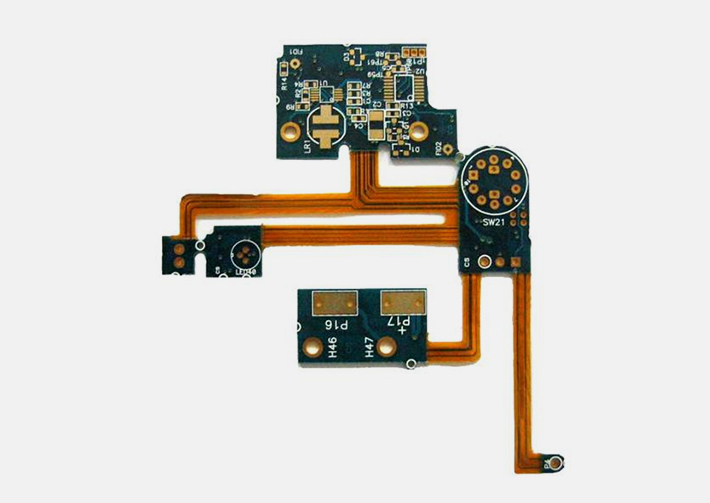
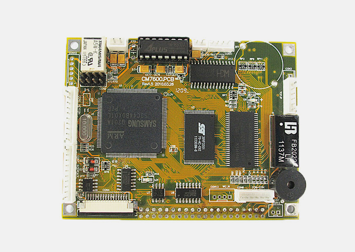
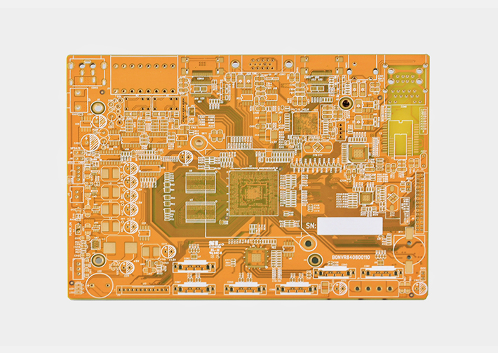
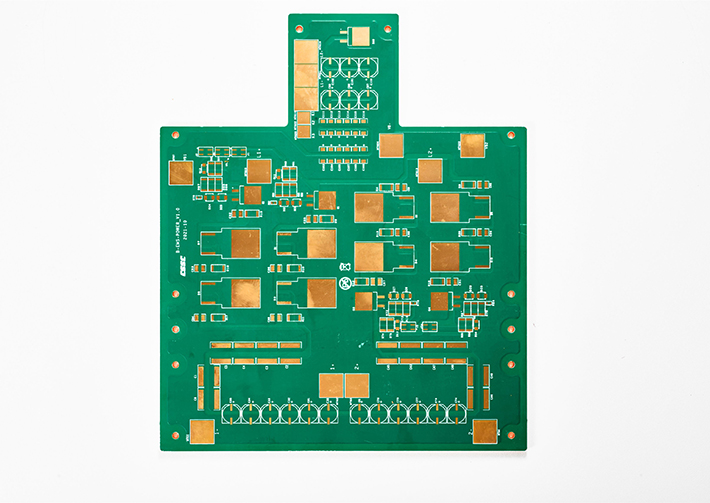
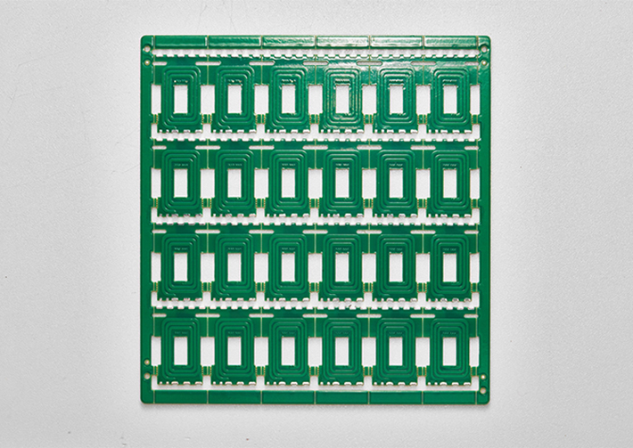
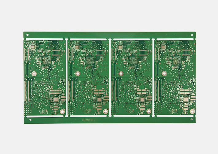
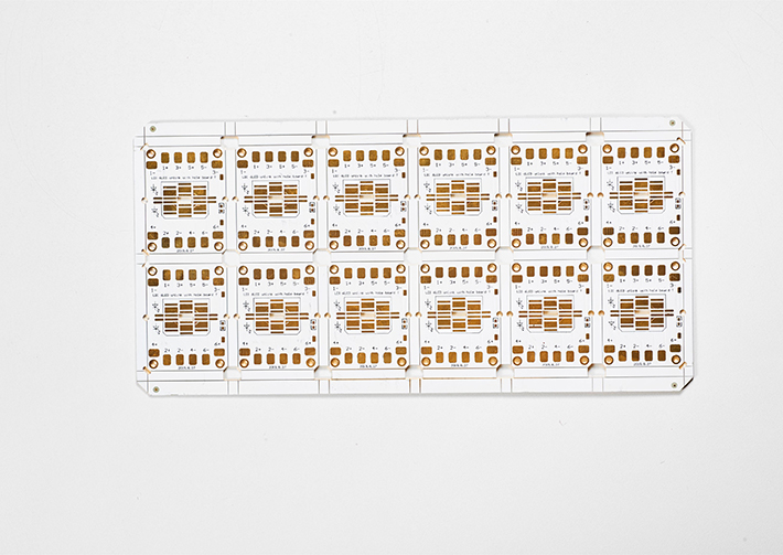
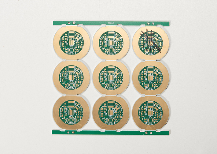
As a leading manufacturer and supplier of printed circuit boards in China, we are proud to introduce our latest product featuring blind and buried vias. Our cutting-edge technology allows us to create intricate PCB designs with ease, giving our customers the flexibility and freedom they need to bring their innovative ideas to life.
Blind vias are used to connect the surface layer of a PCB to an inner layer without penetrating the entire board. This technique minimizes signal interference and allows for more compact circuit designs. Buried vias, on the other hand, are used to connect multiple inner layers without penetrating the outer layers of the board.
Our blind and buried vias product combines the best of both worlds, providing a solution for complex circuit designs that require both types of vias. With our state-of-the-art manufacturing facilities and expert team of engineers, we can customize our product to meet the specific needs of each customer.
We take pride in delivering high-quality PCBs that exceed our customers' expectations. Contact us today to learn more about our blind and buried via PCB solutions.
Shenzhen Omni Pcb Technology Limited Co.,LTD.
Company News
Related News
Aluminum PCB one
Aluminum PCB - We are a factory providing high-quality and durable aluminum printed circuit boards. Trust us for your electronic needs. Contact us now!
Copper PCB 25
Looking for high-quality copper PCBs? Look no further than our factory. Our Copper PCB 25 product name is reliable and durable, perfect for all your PCB needs. Order today!
Double-Sided-Rigid-Flex-PCB
Looking for high-quality double-sided rigid-flex PCBs? Look no further than our factory! We specialize in producing durable and efficient circuit boards that will take your products to the next level. Contact us today to learn more!
Financial Equipment Control Panel
Looking for a reliable financial equipment control panel? Look no further than our factory! We specialize in high-quality equipment that you can trust.
Mother-board-of-security-surveillance-system
Looking for a reliable {Mother-board-of-security-surveillance-system} manufacturer? Look no further than our factory! We offer high-quality products that help keep your property and loved ones safe.
Copper PCB 14
Looking for high-quality Copper PCB 14? Look no further than our factory! We specialize in producing top-notch PCBs designed to meet your unique needs. Order yours today!
Copper PCB 19
Looking for high-quality {Copper PCB 19}? Look no further than our factory. We specialize in producing top-notch PCBs, with a focus on durability, reliability, and performance. Contact us today to learn more.
6Layer-PCB
6Layer-PCB Factory - High-quality printed circuit boards for your electronic needs. Order from a trusted manufacturer. Get your quote today!
GPRS Backstage Control Board
Looking for a reliable GPRS Backstage Control Board? Our factory has got you covered! We specialize in producing high-quality, cost-effective boards that are built to last. Order now and experience the best in control board technology!
Copper PCB 21
We are a factory specializing in the production of Copper PCB 21. Our high-quality products are made for reliability and durability in electronic devices and machinery.
Aluminum PCB two
Introducing our {Aluminum PCB two} - high-quality boards for superior performance! As a factory, we use top-grade materials & cutting-edge tech to ensure excellent results. Choose us for reliable and efficient circuit boards!
HDI-for-industrial-equipment
Boost your manufacturing productivity with HDI-for-industrial-equipment. We are a factory devoted to creating high-quality products that meet your needs.
Copper PCB 26
As a leading Copper PCB 26 factory, we specialize in producing high-quality PCBs that are reliable and cost-effective. Contact us today! #CopperPCB26 #PCBFactory #QualityProducts
Copper PCB 16
Copper PCB 16 now available from our factory. Precision made PCBs with exceptional heat dissipation capabilities. Order now for rapid delivery." #PCBmanufacturer #Copper16 #FastDelivery
Industrial Controller
Looking for a reliable industrial controller for your factory? Look no further than our top-quality products. Achieve greater efficiency and productivity with our innovative solutions.
- Blind and Buried Vias from Leading Manufacturer, Exporter and OEM Supplier in China
- Reviews
Introducing our latest printed circuit board (PCB) technology - the blind via buried via technology. This innovative technology uses advanced procedures to deliver better performance and reliability for your circuit board design and manufacturing needs. The blind via buried via technology involves creating tiny holes or vias on the PCB surface that can be used to connect different layers of the board. These vias are strategically positioned to minimize interference and improve overall electrical performance. This technology is especially useful for high-density circuits where space is limited, and signal integrity is crucial. Using our blind via buried via technology for your PCB designs provides several benefits. For starters, it enhances the board's efficiency, resulting in higher performance. It also minimizes signal reflections, allowing for faster signal speed and reduced electromagnetic interference (EMI). Additionally, this technology also reduces the layer count of your boards, thus-making the design more cost-effective. Our blind via buried via technology can be applied to different PCB designs, from single to multi-layered, allowing for more versatility in circuit board design. With our team's vast experience in designing and manufacturing PCBs, coupled with our state-of-the-art technology, we guarantee you a high-quality product that satisfies your specific needs. Contact us today to learn more about our blind via buried via technology and take advantage of our expertise to improve your PCB design and manufacturing process.
The Blind Via Buried Via is an excellent product that helps to enhance connectivity and improve the performance of printed circuit boards (PCBs). These vias are specifically designed for situations where traditional vias may not work, such as those with tight spacing or dense board designs. They are called blind vias because they only connect to one side of the board, while buried vias only connect to inner layers. The product is easy to use and is suitable for both high and low density boards. It helps to reduce signal loss and improve board reliability while also lowering costs. The technology used to create these vias ensures that they are durable, robust, and precise, making them a popular choice for many PCB design applications. Overall, the Blind Via Buried Via is a reliable and innovative product that helps to solve many connectivity problems that PCB designers may encounter. Its high-quality standards and excellent performance make it an essential tool for any electronic engineer or designer who wants to create high-quality PCBs that deliver superior performance.
Ms. carlen shu
As an electronics enthusiast, I've had the opportunity to work with various printed circuit boards (PCBs) that require Blind and Buried Via features. Recently, I've been using PCB manufacturer, PCBWay, for my projects, and I'm impressed with their quality and affordability. Their Blind Via and Buried Via features are excellent. Their Blind Via technology allows for more complex routing between layers, which is perfect for my designs that require high-density connections. Their Buried Via technology enables me to make more connections on inner layers without compromising on board size. Moreover, PCBWay's fabrication quality is exceptional with high precision and detail to ensure that the via holes are well-made. Overall, I'm satisfied with their products and services, and I highly recommend them for your PCB needs.
Ms. Angela Her
Contact us
Please feel free to give your inquiry in the form below We will reply you in 24 hours

